Device containing cytophilic islands that adhere cells separated by cytophobic regions

a technology of cytophilic islands and cells, applied in the direction of cell culture supports/coatings, immobilised enzymes, chemical vapor deposition coatings, etc., can solve the problems of low surface permeability, low surface permeability, and low surface permeability, and achieve the effect of promoting or preventing cell-cell conta

Inactive Publication Date: 2006-09-21
PRESIDENT & FELLOWS OF HARVARD COLLEGE
View PDF4 Cites 46 Cited by
  • Summary
  • Abstract
  • Description
  • Claims
  • Application Information

AI Technical Summary

Problems solved by technology

While the above-described irradiative lithographic methods may be advantageous in many circumstances, all require relatively sophisticated and expensive apparatus to reproduce a particular material pattern on a plurality of substrates, and are relatively time-consuming.
Additionally, no method of patterning other than on a flat substrate is commonly available according to the methods.

Method used


Image

  • Device containing cytophilic islands that adhere cells separated by cytophobic regions
  • Device containing cytophilic islands that adhere cells separated by cytophobic regions

Examples


example 1

Preparing a Mold and Stamp

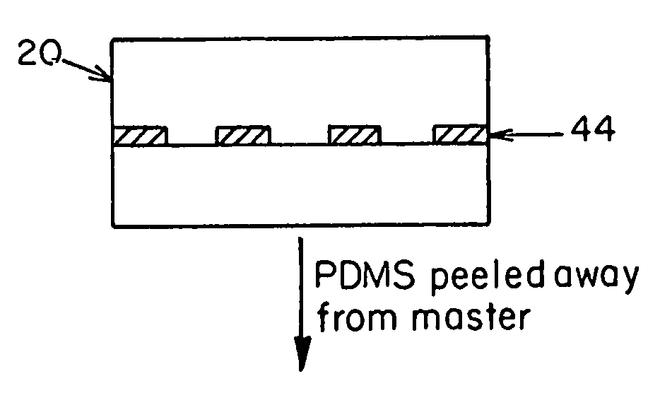
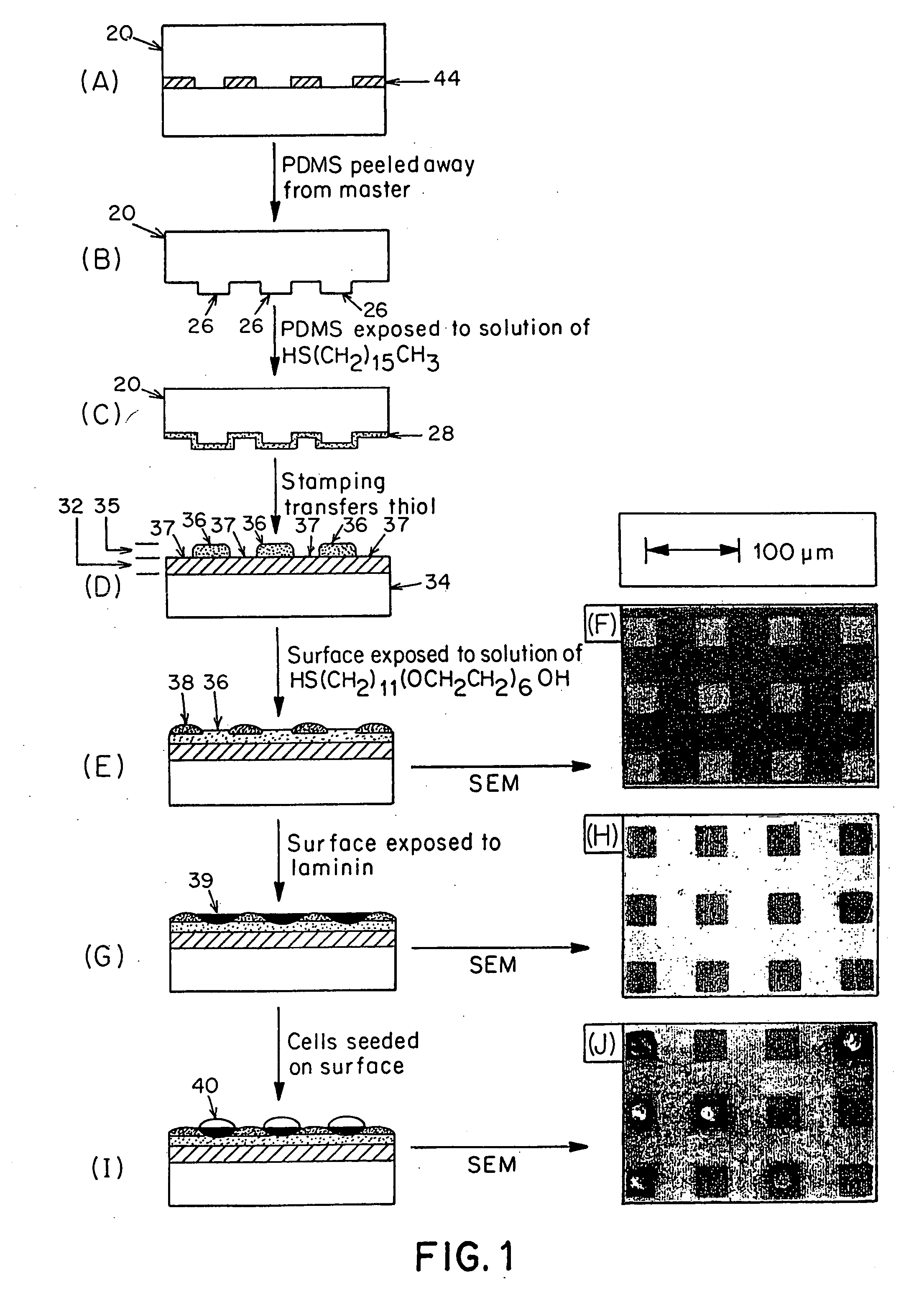
[0097] A mold according to the present invention was fabricated. A template consisting of an exposed and developed photoresist pattern on silicon is prepared (This type of fabrication is described in any conventional photolithography text, such as Introduction to Microelectronic Fabrication, by Richard C. Jaeger, Gerold W. Neudeck and Robert F. Pierret, eds., Addison-Wesley, 1989). Templates such as electron microscopy grids or other corrugated materials may also be used. The template is placed in a container such as a petri dish. A 10:1 (w:w or v:v) mixture of PDMS-Sylgard Silicone Elastomer 184 and Sylgard Curing Agent 184 (Dow Coming Corp., Midland, Mich.) was poured into the petri dish. It was not necessary to put the mixture of PDMS-elastomer and curing agent under vacuum to remove dissolved dioxygen. The PDMS cured at room temperature in the laboratory ambient for 30 to 60 min. This cure was followed by additional curing at 65° C. for approximately o...

example 2

Preparation of Plates with Metallic Surfaces

[0098] Gold films (˜2000 A thick) were prepared by electron-beam evaporation of gold (Materials Research Corp., Orangeburg, N.Y.; 99.999%) onto single-crystal silicon (100) test wafers (Silicon Sense, Nashua, N.H.; 100 mm dia., ˜500 μm thick) that had been precoated with a film of titanium (Johnson Mathey, 99.99%; ˜50 A thick) that acted as an adhesion promoter between the silicon oxide and the gold. The silicon wafers coated with gold were fractured into square plates (˜2 cm×2 cm) and used in the formation of the various types of patterned SAM plates.

example 3

Preparing a Patterned Plate with a Grid Pattern

[0099] A stamp fabricated in accordance with Example 1 was fabricated. The stamp was fabricated so as to have a linear indentation pattern contiguous with a liner stamping surface pattern. That is, the stamp had an array of indentational lines separating stamping surface lines. The surface was coated with hexadecanethiol in ethanol using a cotton swab. The stamp was applied to a smooth gold surface, and removed. The resultant pattern included parallel SAM lines of 2 microns in width. After removal of the stamp, the stamping surface was re-coated and rotated approximately 45° to a second orientation, and re-applied to the surface. A grid pattern resulted.


PUM

PropertyMeasurementUnit
areaaaaaaaaaaa
areaaaaaaaaaaa
timeaaaaaaaaaa

Abstract

The invention provides a device for adhering cells in a specific and predetermined position, and associated methods. The device includes a plate defining a surface and a plurality of cytophilic islands that adhere cells, isolated by cytophobic regions to which cells do not adhere, contiguous with the cytophilic islands. The islands or the regions or both may be formed of a self-assembled monolayer (SAM).

Description

RELATED APPLICATIONS [0001] This application is a continuation of U.S. patent application Ser. No. 10 / 032,280, filed Dec. 21, 2001 which is a continuation of copending U.S. patent application Ser. No. 09 / 373,334, filed Aug. 12, 1999, which is a continuation of U.S. patent application Ser. No. 08 / 951,886, filed Oct. 16, 1997, which is a continuation of U.S. patent application Ser. No. 08 / 659,537, filed Jun. 7, 1996, now U.S. Pat. No. 5,776,748, which is a continuation of U.S. patent application Ser. No. 08 / 131,838 filed Oct. 4, 1993.[0002] This invention was made with government support NSF Grant Number EEC-880-3014, NIH Grant Number GM30367, ONR Grant Number N00014-86-K-0756, and ACS Grant Number CD-493. The government has certain rights to the invention.FIELD OF THE INVENTION [0003] The present invention relates generally to derivatization and patterning of surfaces, more particularly to the formation on surfaces of patterns of self-assembled molecular monolayers with differing bio...

Claims


Application Information

Patent Timeline
Patent Type & Authority Applications(United States)
IPC IPC(8): A61F2/06A61F13/00B01J19/00B81C1/00C12N5/00C12N5/02C12N5/071C40B60/14
CPCB01J19/0046B01J2219/00382B01J2219/00385B01J2219/00585B01J2219/00596B01J2219/00605B01J2219/0061B01J2219/00612B01J2219/00617B01J2219/00619B01J2219/00621B01J2219/00626B01J2219/0063B01J2219/00637B01J2219/00659B01J2219/0072B81B2201/0214B81C1/00206B81C2201/034B82Y5/00B82Y30/00C12N5/0068C12N5/067C12N2535/10C40B60/14C12Q1/02C12N1/00
Inventor SINGHVI, RAHULKUMAR, AMITWHITESIDES, GEORGE M.INGBER, DONALD E.LOPEZ, GABRIEL P.WANG, DANIEL I. C.STEPHANOPOULOS, GREGORY N.
Owner PRESIDENT & FELLOWS OF HARVARD COLLEGE
Why Eureka
Try Eureka