Imaging device

a technology of image processing and photodiodes, applied in the field of image processing devices, can solve the problems of not being able to store more charge than the storage capacity, not being able to receive all the generated charge transferred from a photodiode, and not being able to compare techniques to set an individual accumulation period for each pixel group

Active Publication Date: 2017-09-07
RICOH KK
View PDF0 Cites 1 Cited by
  • Summary
  • Abstract
  • Description
  • Claims
  • Application Information

AI Technical Summary

Problems solved by technology

However, such comparative techniques does not set an individual accumulation period for each pixel group and keep the condition of the floating diffusion at a certain level at the time of starting the transfer of charge.
If charge is transferre

Method used


Image

  • Imaging device
  • Imaging device
  • Imaging device

Examples


Embodiment Construction

[0019]The terminology used herein is for the purpose of describing particular embodiments only and is not intended to be limiting of the present invention.

[0020]As used herein, the singular forms “a”, “an” and “the” are intended to include the plural forms as well, unless the context clearly indicates otherwise.

[0021]In describing preferred embodiments illustrated in the drawings, specific terminology may be employed for the sake of clarity. However, the disclosure of this patent specification is not intended to be limited to the specific terminology so selected, and it is to be understood that each specific element includes all technical equivalents that have the same function, operate in a similar manner, and achieve a similar result.

[0022]An embodiment of the present invention will be described in detail below with reference to the drawings.

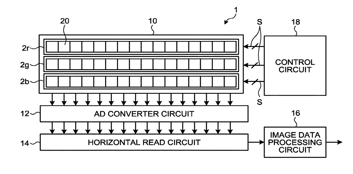
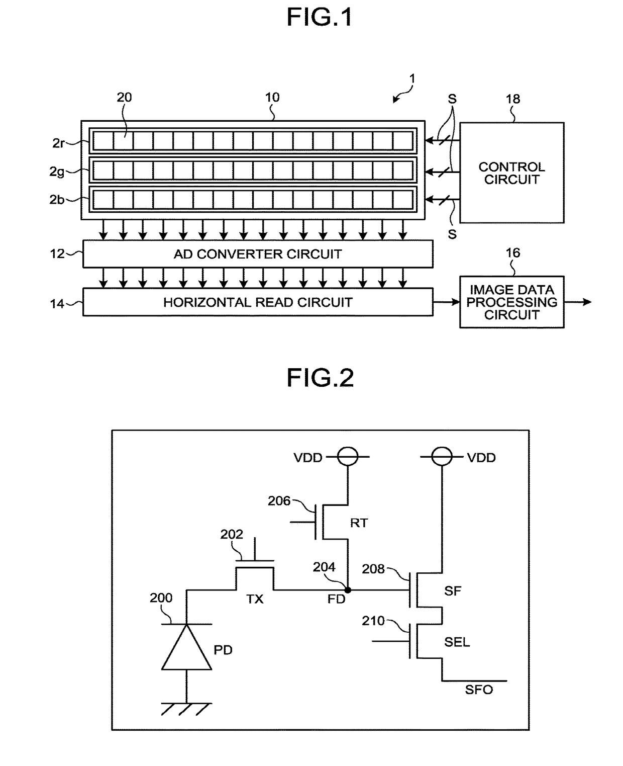
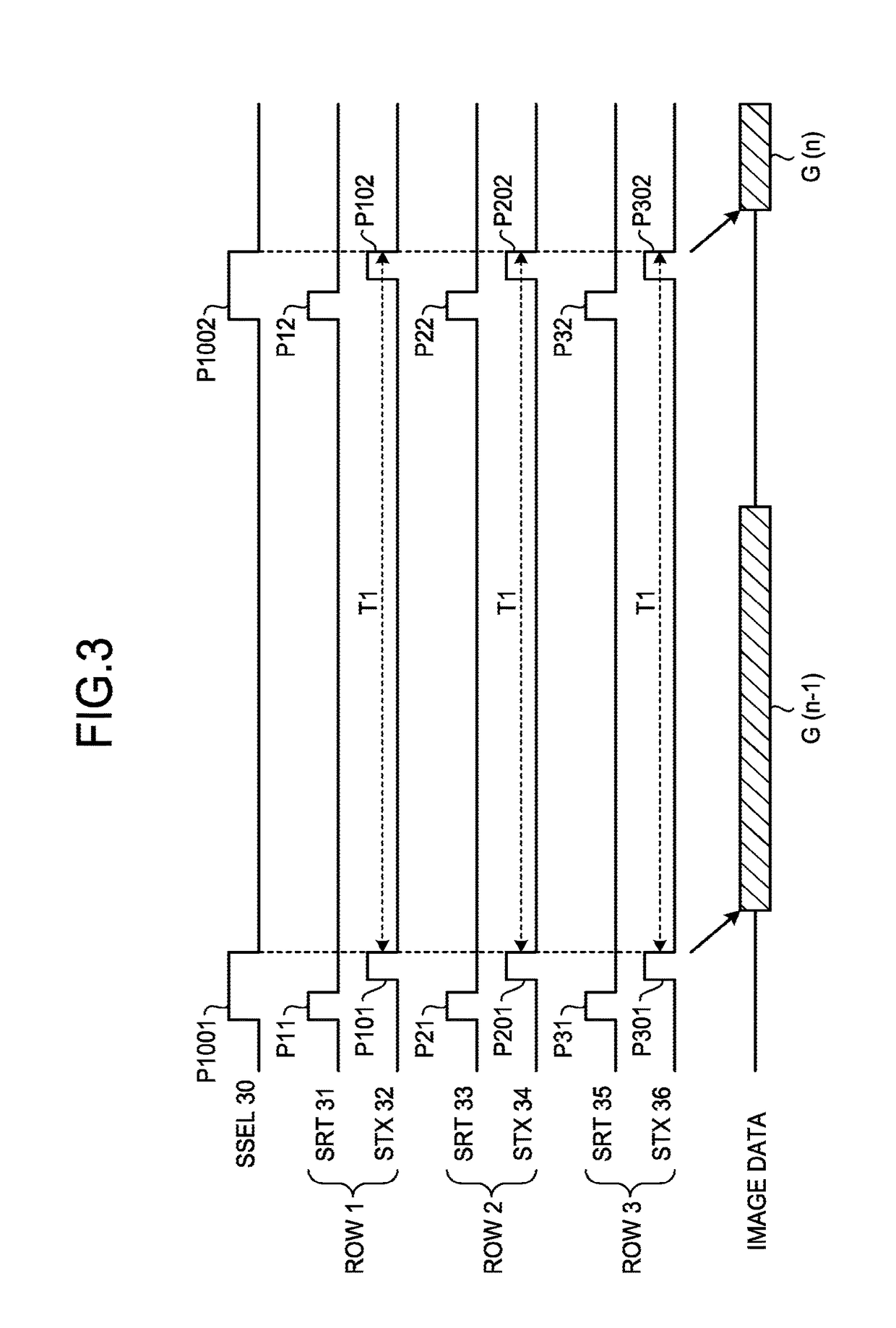
[0023]An embodiment has an object to provide an imaging device that can correct differences in pixel sensitivity among pixel groups and can r...


PUM


Abstract

An imaging device includes a plurality of arranged imaging elements each including: a light-receiving element configured to generate charge from received light by photoelectric conversion, a floating diffusion configured to convert the charge generated by the light-receiving element into voltage, a charge transfer switch configured to transfer the charge from the light-receiving element to the floating diffusion, a reset switch configured to reset the voltage of the floating diffusion, and a source follower configured to amplify the voltage of the floating diffusion. The reset switch is configured to reset the voltage of the floating diffusion a plurality of times for each of predetermined pixel groups in a single image data acquisition period. The charge transfer switch is configured to transfer the charge from the light-receiving element to the floating diffusion a plurality of times for each of the pixel groups in the single image data acquisition period.

Description

CROSS-REFERENCE TO RELATED APPLICATIONS[0001]The present application claims priority under 35 U.S.C. §119 to Japanese Patent Application No. 2016-039073, filed Mar. 1, 2016, and Japanese Patent Application No. 2016-254058, filed Dec. 27, 2016. The contents of which are incorporated herein by reference in their entirety.BACKGROUND OF THE INVENTION[0002]1. Field of the Invention[0003]The present invention relates to an imaging device.[0004]2. Description of the Related Art[0005]Imaging devices such as complementary metal oxide semiconductor (CMOS) linear image sensors read image data at certain rates. For example, a photodiode in each pixel accumulates charge by photoelectric conversion and the accumulated charge is transferred to a floating diffusion at certain timing, and the charge retained in the floating diffusion is read as image data. The following describes examples of pixel data read-out techniques of comparative imaging devices.[0006]For example, Japanese Unexamined Patent A...

Claims


Application Information

Patent Timeline
IPC IPC(8): H01L27/146H01L27/148H04N5/378H04N9/04H04N5/374
CPCH01L27/14645H04N9/045H01L27/14868H04N5/378H04N5/374H04N25/533H04N25/534H04N25/626H04N23/84H04N25/76
Inventor SAKAGUCHI, SHINJIKANNO, TOHRU
Owner RICOH KK
Why Eureka
Try Eureka