Package substrate with double sided fine line rdl

a technology of fine line and packaging substrate, applied in the field of packaging substrate, can solve the problem of weak signal receiving

Active Publication Date: 2017-09-14
HU DYI CHUNG
View PDF0 Cites 6 Cited by
  • Summary
  • Abstract
  • Description
  • Claims
  • Application Information

AI Technical Summary

Benefits of technology

[0009]A package substrate has a middle redistribution layer functions as a core redistribution layer. The middle redistribution layer is sandwiched by a top redistribution layer and a bottom redistribution layer. A top surface of the top redistribution layer has a plurality of top metal pads adaptive for at least one chip to mount, and a bottom surface of the bottom redistribution layer has a plurality of bottom metal pads adaptive for at least one chip to mount, a compact system in package can be achieved. The neighbored chips communicate with each other through a shorter circuitry and the top bottom neighbored chips also communicate with a shorter circuitry. A flexible circuit board is prepared, the flexible circuit board has electrical circuity thereon. The circuitry of the flexible circuit board has a first end electrically coupled to the second circuitry of the second redistribution layer and has a second end electrically coupled to system board or additional electronic devices.

Problems solved by technology

The disadvantage for the prior art is that the longer the path it goes, the weaker the signal is received.

Method used


Image

  • Package substrate with double sided fine line rdl
  • Package substrate with double sided fine line rdl
  • Package substrate with double sided fine line rdl

Examples


first embodiment

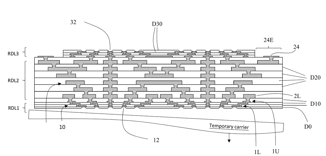
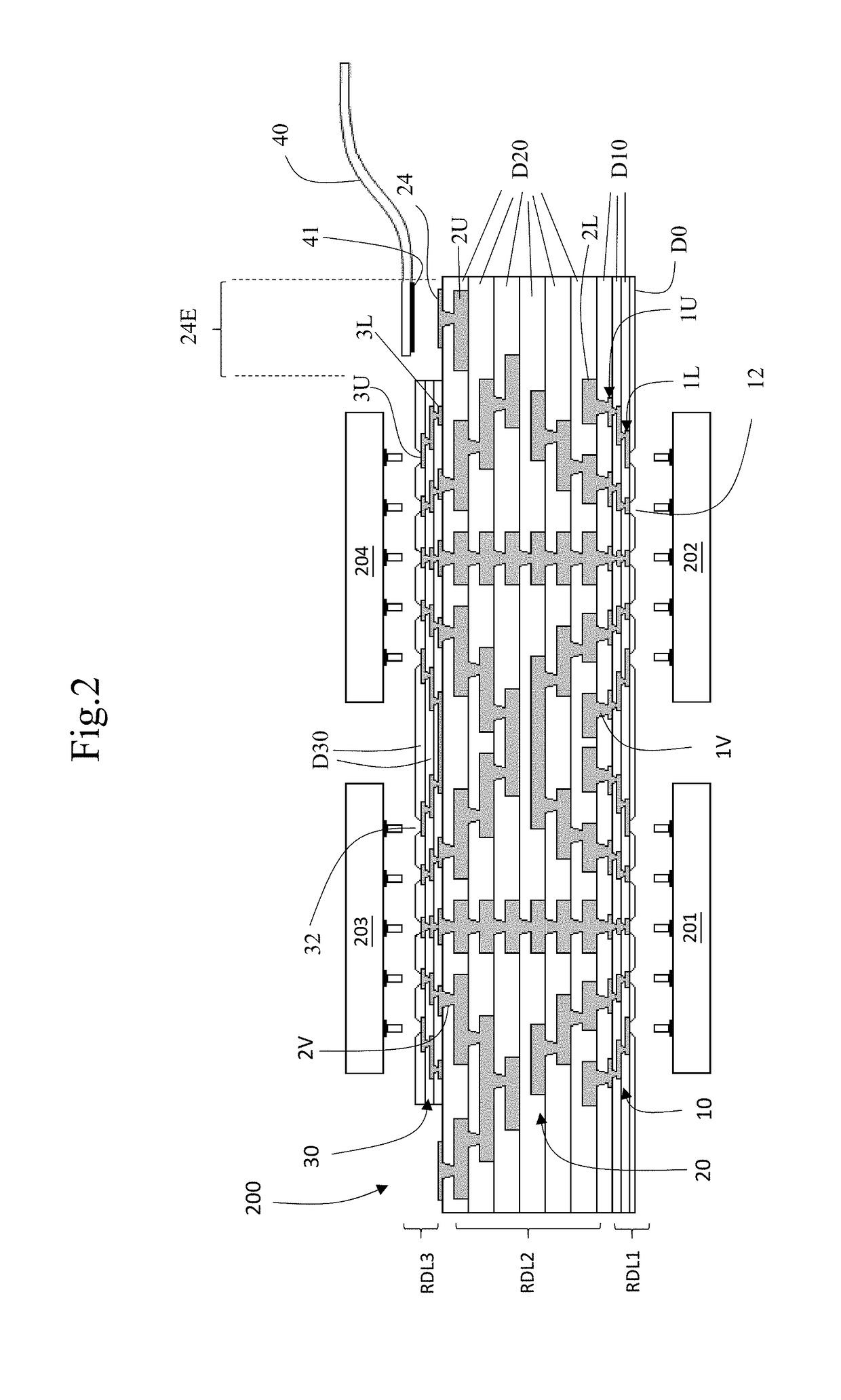
[0010]FIG. 2 shows a first embodiment according to the present invention.

[0011]FIG. 2 shows a package substrate 200 which has a middle redistribution layer RDL2. The middle redistribution layer RDL2 is sandwiched by a bottom redistribution layer RDL1 and a top redistribution layer RDL3.

[0012]The first redistribution layer RDL1 is fabricated according semiconductor process. The first redistribution layer RDL1 has a first circuitry 10 embedded in a plurality of first dielectric layers D10; the first circuitry 10 comprises a plurality of first upper metal pads 1U configured on a top side of the first redistribution layer RDL1, and a plurality of first lower metal pads 1L configured on a bottom side of the first redistribution layer RDL1; a density of the first lower metal pads 1L is higher than a density of the first upper metal pads 1U; a bottom side of the first lower metal pads 1L is adaptive to mount at least one chip; a first chip 201 and a second chip 202 are, for example, mounte...


PUM


Abstract

A package substrate has a sandwiched redistribution layers is disclosed. A middle redistribution layer functions as a core redistribution layer sandwiched by a top redistribution layer and a bottom redistribution layer. A top surface of the top redistribution layer is made adaptive for at least one chip to mount, and a bottom surface of the bottom redistribution layer is made adaptive for at least one chip to mount. A line width of each circuit of the middle redistribution layer is wider than a circuit of either the top redistribution layer or the bottom redistribution layer.

Description

BACKGROUND[0001]Technical Field[0002]The present invention relates to a package substrate, especially relates to a package substrate with double sided fine line redistribution layer (RDL) for a system in package. The top side of the package substrate is made adaptive to mount at least one chip thereon. The bottom side of the package substrate is made adaptive to mount at least one chip thereon. The line width of a metal circuit of the middle redistribution layer is wider than a line width of a metal circuit of the top redistribution layer, and the line width of a metal circuit of the middle redistribution layer is wider than a line width of a metal circuit of the bottom redistribution layer.[0003]Description of Related Art[0004]FIG. 1 shows a prior art.[0005]FIG. 1 shows that a first chip 501 and a second chip 502 are configured on a top side of an interposer 51. The interposer 51 is configured on a top side of a package substrate 52. The package substrate 52 is configured on a syst...

Claims


Application Information

Patent Timeline
Patent Type & Authority Applications(United States)
IPC IPC(8): H01L23/00H01L21/48H01L23/498
CPCH01L24/02H01L23/498H01L24/06H01L23/49827H01L2224/0612H01L2224/02373H01L2224/0231H01L2224/02331H01L21/4846H01L21/4853H01L23/49816H01L23/49838H01L21/6835H01L25/0655H01L2221/68345H01L2224/16237H01L2224/81191H01L23/4985H01L23/5383H01L25/0652H01L25/50
Inventor HU, DYI-CHUNG
Owner HU DYI CHUNG
Why Eureka
Try Eureka