

Stacked chip package structure and manufacturing method thereof
a technology of stacking and chip, applied in the direction of semiconductor devices, electrical devices, semiconductor/solid-state device details, etc., can solve the problems of disadvantageous damage to devices including semiconductor chips, and achieve the effects of reducing production costs, reducing production costs, and reducing overall thickness
- Summary
- Abstract
- Description
- Claims
- Application Information
AI Technical Summary
Benefits of technology
Problems solved by technology
Method used
Image

Examples
Embodiment Construction
[0012]Reference will now be made in detail to the present preferred embodiments of the invention, examples of which are illustrated in the accompanying drawings. Wherever possible, the same reference numbers are used in the drawings and the description to refer to the same or like parts.
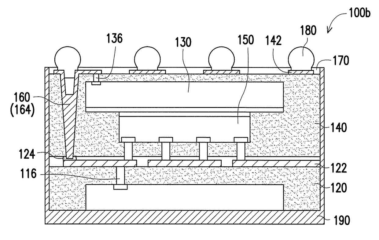
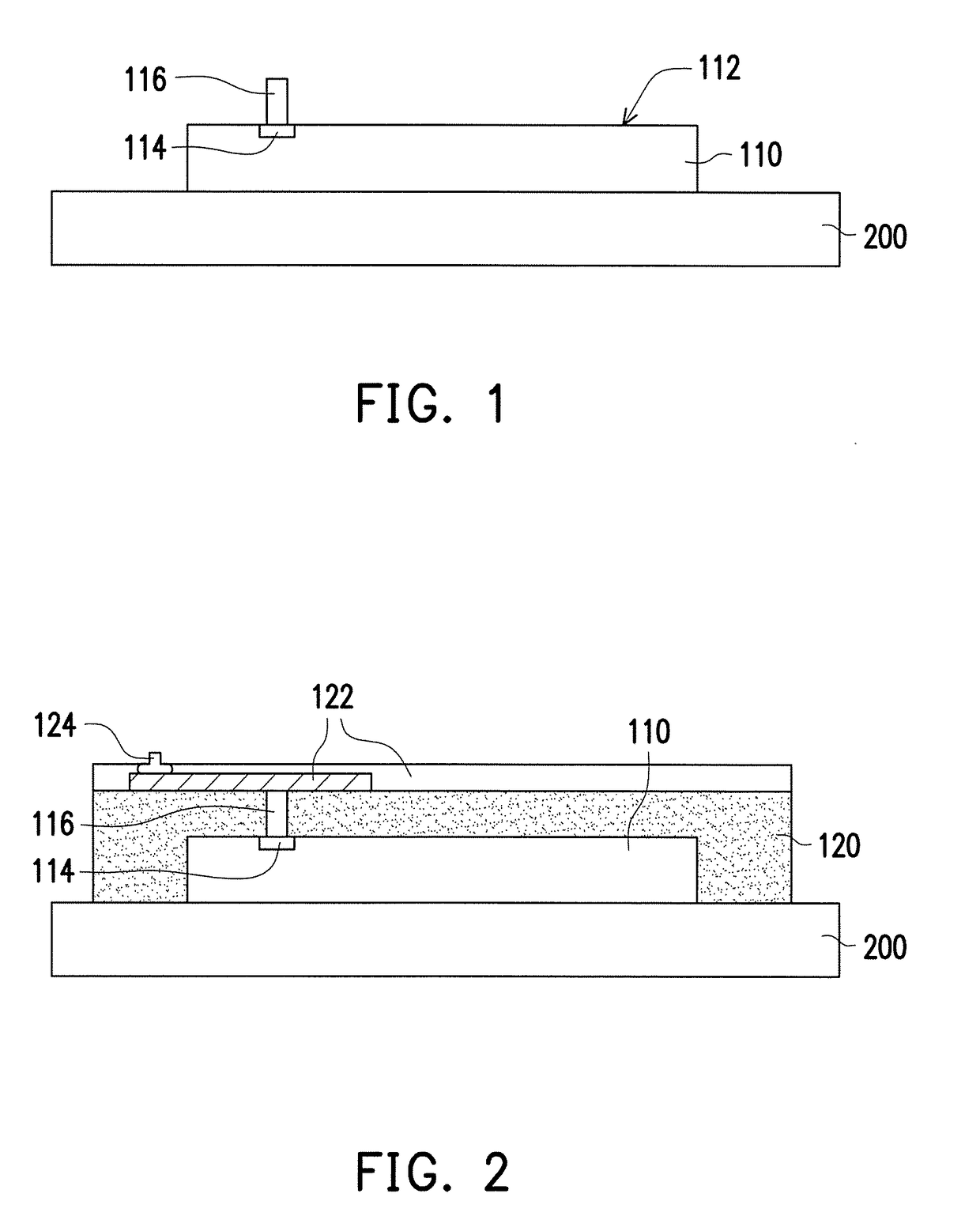
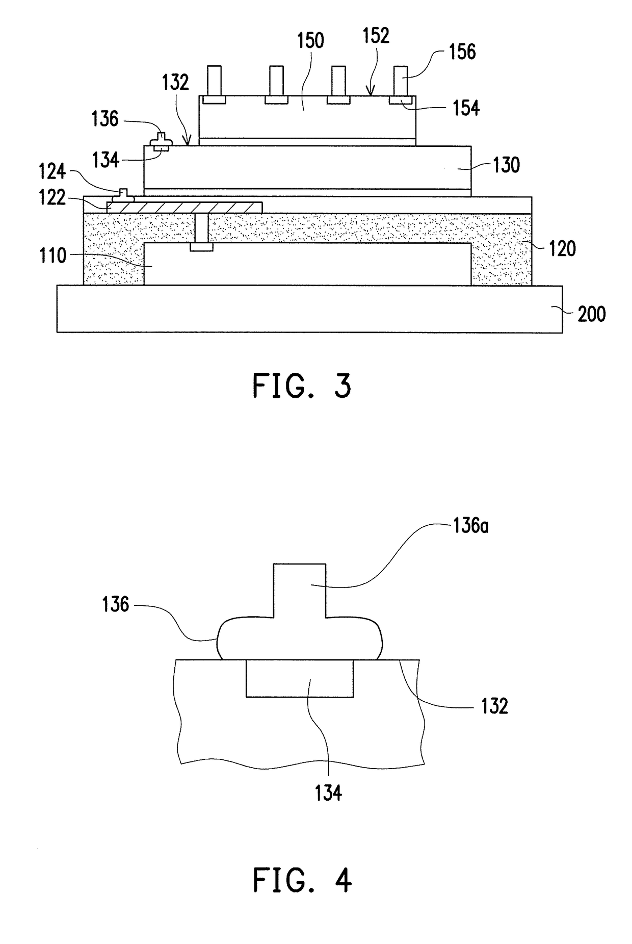
[0013]FIG. 1 to FIG. 9 illustrate cross-sectional views of a manufacturing process of a stacked chip package structure according to an embodiment of the invention. In the present embodiment, a manufacturing process of a stacked chip package structure may include the following steps. Referring to FIG. 1 and FIG. 2, a first chip 110 is firstly disposed on a carrier 200. The first chip 110 includes a first active surface 112 facing away from the carrier 200 and a plurality of first pads 114 disposed on the first active surface 112. Then, a plurality of first pillar bumps 116 are correspondingly formed on the first pads 114 respectively. The first pillar bumps 116 may be formed by screen printing or elec...
PUM
 Abstract
Description
Claims
Application Information