

Display device
- Summary
- Abstract
- Description
- Claims
- Application Information
AI Technical Summary
Benefits of technology
Problems solved by technology
Method used
Image

Examples
first embodiment
1. First Embodiment
[0127]
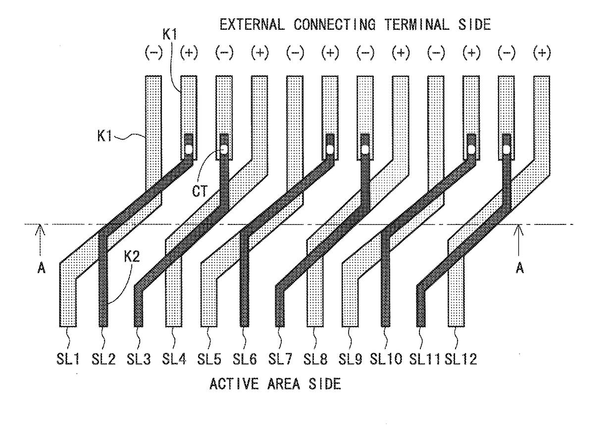
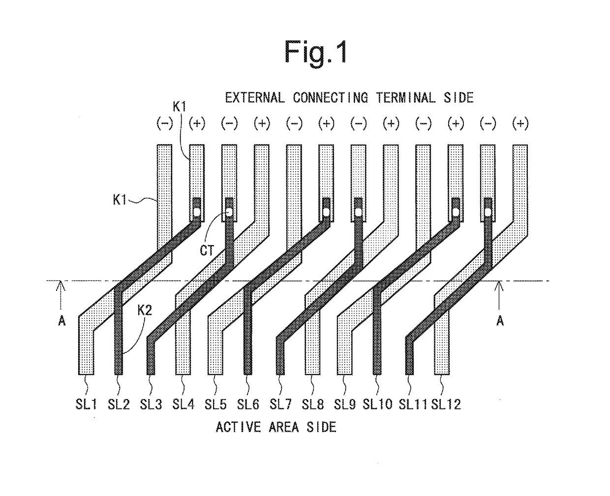
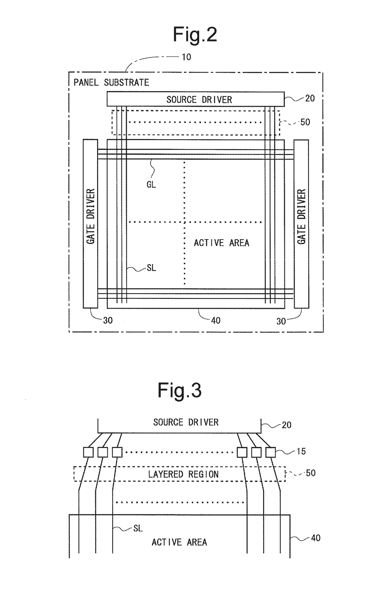
[0128]FIG. 2 is a block diagram illustrating an entire configuration of an active matrix-type liquid crystal display device according to a first embodiment of the present invention. As illustrated in FIG. 2, this liquid crystal display device is provided with a source driver 20, a gate driver 30, and an active area (display region) 40. The active area 40 and the gate driver 30 are provided on a panel substrate 10. Here, the panel substrate 10 in this embodiment is a glass substrate. The source driver 20 is mounted on the panel substrate 10 in a COG (Chip On Glass) manner, for example. Specifically, the source driver 20 in this embodiment is an IC chip. On the panel substrate 10, external connecting terminals for receiving video signals output from the source driver 20 which is an IC chip are provided. Here, a region indicated by a reference character 50 in FIG. 2 is a region having a layered wiring structure (hereinafter referred to as a “layered region”). A...
second embodiment
2. Second Embodiment
[0190]Next, a second embodiment of the present invention will be described. Here, a description of a part similar with the first embodiment will be omitted. Regarding the polarity reversal method, the description is given assuming that the one-column reversal driving method is employed. However, a multi-column reversal driving method may be employed, or the dot-reversal driving method may be employed.
[0191]
[0192]A description for an entire configuration will be omitted since the configuration is the same as that of the first embodiment (see FIG. 2). FIG. 39 is a plan view illustrating a wiring structure (a wiring structure between the external connecting terminals 15 and the active area 40) of the layered region 50 according to this embodiment. As illustrated in FIG. 39, the liquid crystal display device according to this embodiment is provided with two layered regions (a first layered region 50a and a second layered region 50b). A cross-sectional view of the fir...
third embodiment
3. Third Embodiment
[0203]Next, a third embodiment of the present invention will be described. Note that, a region in which wiring is not layered (a region other than the layered region 50) is hereinafter referred to as a “non-layered region” for convenience sake.
[0204]
[0205]FIG. 45 is a block diagram illustrating an entire configuration of the active matrix-type liquid crystal display device according to this embodiment. The liquid crystal display device according to this embodiment is provided with a testing circuit 60, in addition to the components of the first embodiment. The testing circuit 60 is provided in a region between the active area 40 and the layered region 50. The testing circuit 60 examines whether or not there is leakage between adjacent source bus lines SL. The components other than the testing circuit 60 are the same as those of the first embodiment, and therefore a description for these components will be omitted. Here, it is assumed that the wiring structure of t...
PUM
 Abstract
Description
Claims
Application Information