Techniques for Forming FINFET Transistors with Same Fin Pitch and Different Source/Drain Epitaxy Configurations
- Summary
- Abstract
- Description
- Claims
- Application Information
AI Technical Summary
Benefits of technology
Problems solved by technology
Method used
Image

Examples
Embodiment Construction
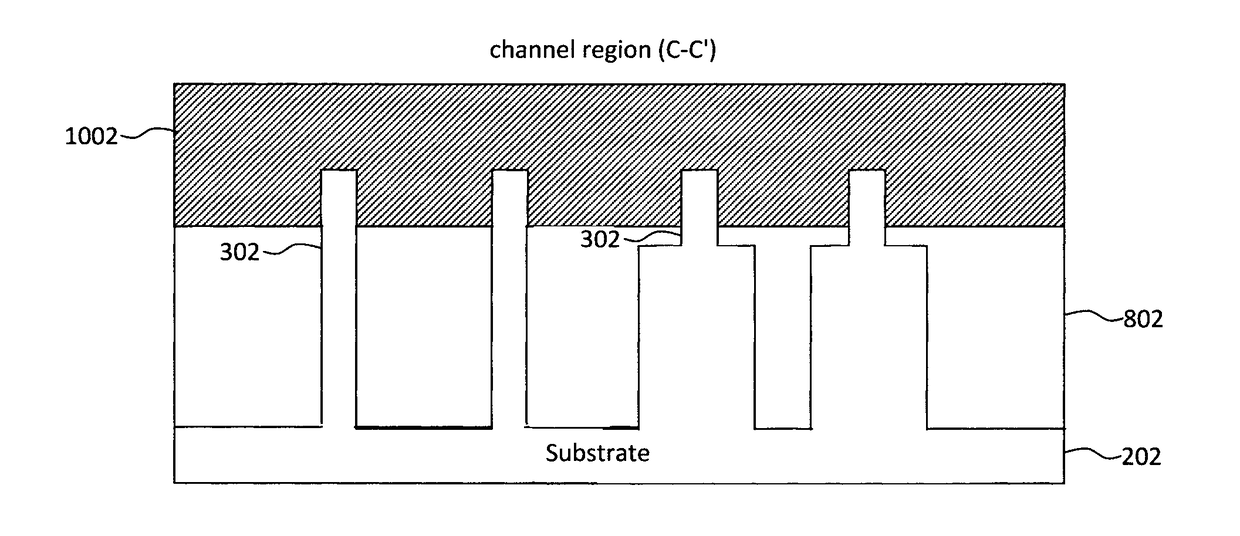
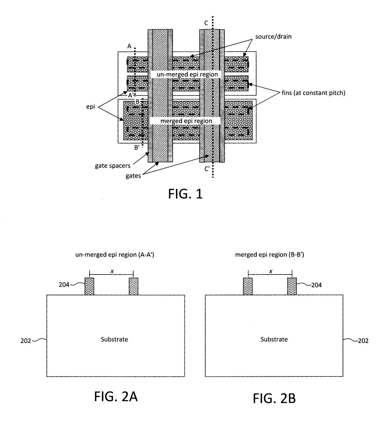
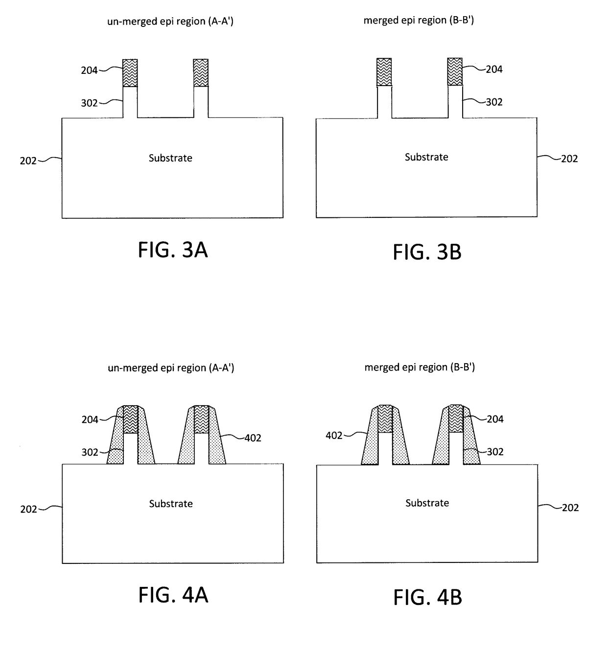
[0037]Provided herein are techniques for forming fin field effect transistor (finFET) devices having different source / drain epitaxy (i.e., un-merged and merged source / drain epitaxy) using the same process and having the same fin pitch. Advantageously, the present process enables the formation of finFET transistors for which it is desirable to have merged epitaxy (such as with logic transistors) and those for which it is desirable to have un-merged epitaxy (such as with SRAM) using the same process. The process employs the same fin pitch for both types of devices, and therefore there are no density tradeoffs (see above).
[0038]An exemplary process flow implementing the present techniques for forming finFET transistors with a same fin pitch and different source / drain epitaxy configurations is now described by way of reference to FIGS. 1-12. In general, a finFET includes a source region and a drain region connected by at least one fin-shaped channel region. A gate regulates current flow...
PUM
 Abstract
Description
Claims
Application Information