Substrate having pattern and method for manufacturing the same, and semiconductor device and method for manufacturing the same

a semiconductor and pattern technology, applied in non-linear optics, instruments, optics, etc., can solve the problems of easy short circuit with adjacent antennas, uneven surface, uneven surface, etc., and achieve low inductance variation, large electromotive force, and high yield

Inactive Publication Date: 2006-08-03
SEMICON ENERGY LAB CO LTD
View PDF68 Cites 33 Cited by
  • Summary
  • Abstract
  • Description
  • Claims
  • Application Information

AI Technical Summary

Benefits of technology

[0011] In view of the foregoing, the present invention provides a method for manufacturing a substrate having a pattern, which is capable of controlling the distance between adjacent film patterns. The present invention also provides a method for manufacturing a substrate having a pattern which is capable of controlling the width between the film patterns, particularly with a narrow

Problems solved by technology

In addition, surfaces of the composition have different film thicknesses corresponding to the opening portions of the mask, and the surfaces are uneven.
In addition, the surface is uneven.
In a

Method used


Image

  • Substrate having pattern and method for manufacturing the same, and semiconductor device and method for manufacturing the same
  • Substrate having pattern and method for manufacturing the same, and semiconductor device and method for manufacturing the same
  • Substrate having pattern and method for manufacturing the same, and semiconductor device and method for manufacturing the same

Examples


embodiment 1

[0070] In the present embodiment, a width of a film pattern in the case of applying and baking a conductive composition by using a screen printing plate that has an emulsion provided with opening portions having different width with each other will be described with the reference to FIG. 16. Here, as a substrate, two types of a glass substrate and a glass substrate having a film in which silicon and oxygen are combined and an inactive group is combined with the silicon are used. As the conductive composition, Ag paste (manufactured by Sumitomo Electric Industries, Ltd., product name: AGEP-201X) (including silver particles, 2-(2-butoxyethoxy)ethyl acetate, and an epoxy resin) is used. In addition, a screen printing plate in which a wire netting thickness is 14 μm and a width of the opening portion of the wire netting is 53 μm, is used. The width of the opening portions of the emulsion in the screen printing plate is set between 30 μm to 180 μm for every 10 μm.

[0071] A method for man...

embodiment 2

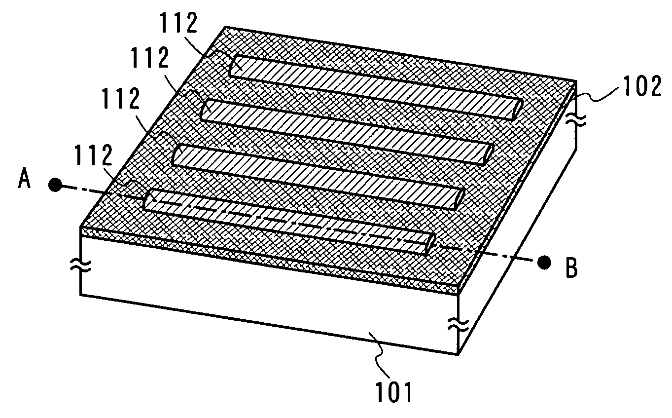
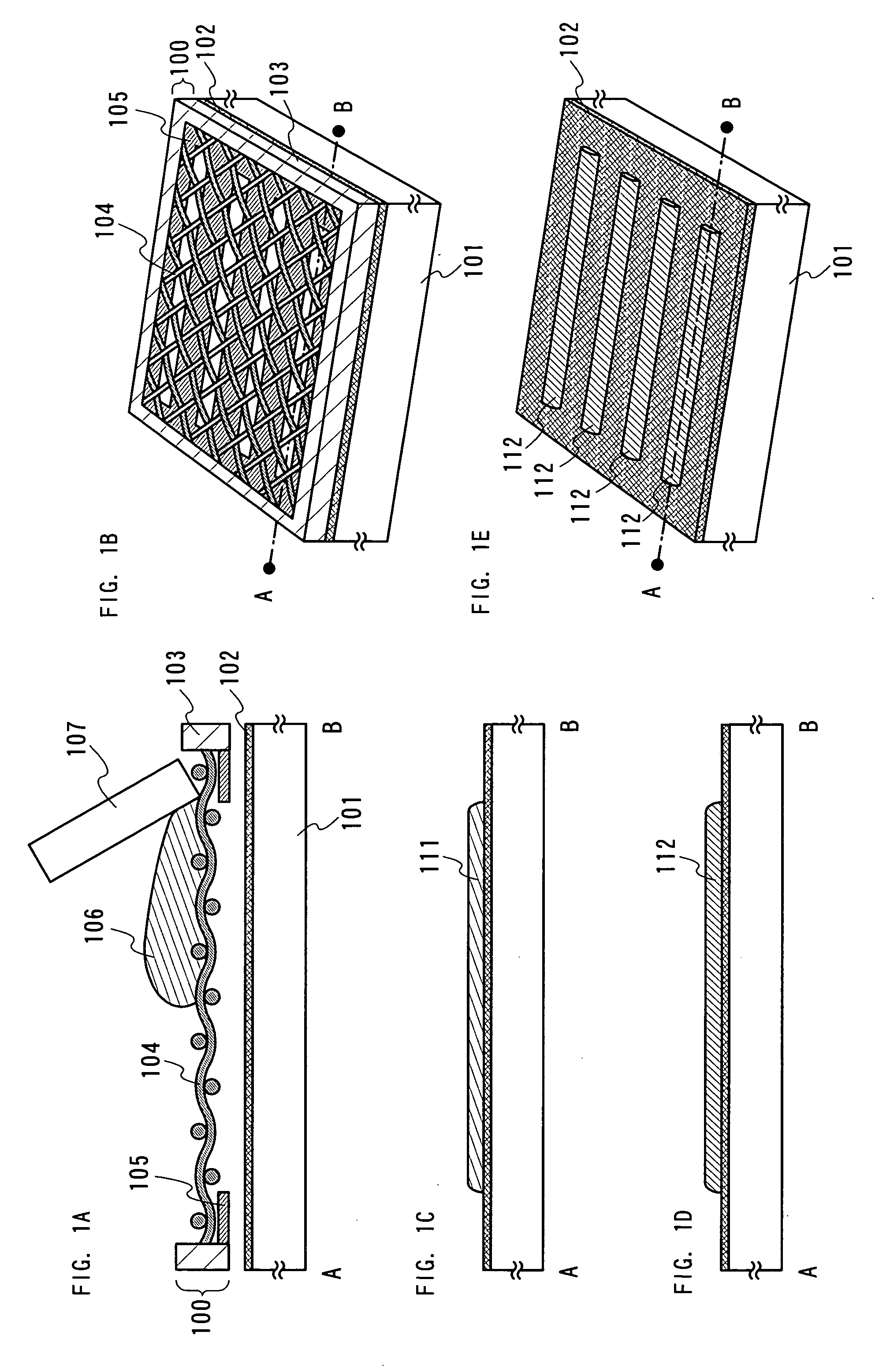
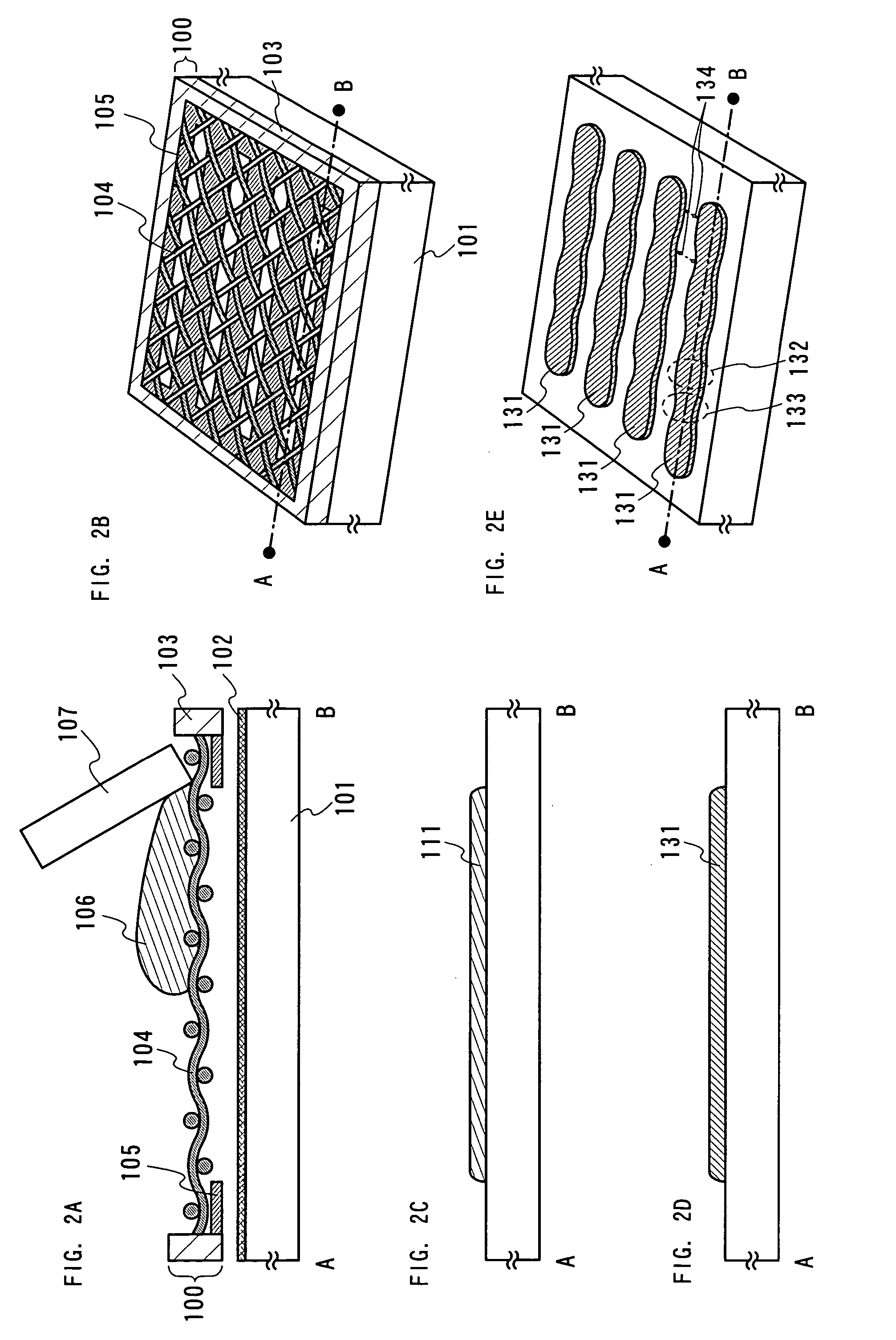
[0088] In the present embodiment, steps of forming a film pattern having conductivity and a semiconductor device having the film pattern according to the present invention will be described with the reference to FIGS. 3A to 3E. As the semiconductor device, semiconductor devices such as a wireless chip, a wireless tag, a wireless IC, an RFID, and an IC tag are used for description. In addition, in the present embodiment, as the film pattern having conductivity, an antenna that is capable of receiving and transmitting data wirelessly is used for description.

[0089]FIGS. 3A, 3C, and 3D show cross-sectional views of a substrate having an antenna. FIGS. 3B and 3E show perspective views of the substrate having the antenna. In addition, FIG. 3A shows the cross-sectional view taken along A-B in FIG. 3B, and FIG. 3D shows the cross-sectional view taken along A-B in FIG. 3E.

[0090] A film 102 in which silicon and oxygen are combined and an inactive group is combined with the silicon is formed...

embodiment 3

[0114] In the present Embodiment, steps of forming a conductive film pattern and a semiconductor device having the film pattern according to the present invention is described with the reference to FIGS. 6A to 6C and FIGS. 7A to 7H. The present embodiment is described by using a pixel electrode as the conductive film pattern and by using a light-emitting display device as the semiconductor device.

[0115]FIG. 6A shows a top view of a pixel portion before sealing. FIG. 6B shows a cross-sectional view taken along A-A′ in FIG. 6A, and FIG. 6C shows a cross-sectional view taken along B-B′ in FIG. 6A.

[0116] A film 212 including silicon, oxygen, and an inactive group is formed over a first substrate 210, and a plurality of first electrodes 213 are arranged in stripe shape with regular distances thereover. A partition wall 214 having an opening portion corresponding to each pixel is provided over each of the first electrodes 213. The partition wall 214 having an opening portion is made of ...


PUM

PropertyMeasurementUnit
Thicknessaaaaaaaaaa
Electrical inductanceaaaaaaaaaa
Electrical conductoraaaaaaaaaa

Abstract

The present invention provides a method for manufacturing a substrate having a pattern that is capable of controlling the distance between adjacent film patterns, and also provides a method for manufacturing a substrate, particularly, having a pattern with a narrow width and a thickness that is capable of controlling the width between the film patterns. The present invention provides a method for manufacturing a substrate having a conductive film that serves as an antenna with a little variation in inductance and has a large electromotive force, and provides a method for manufacturing a semiconductor device with high yield. After forming a film in which silicon and oxygen are combined and an inactive group is combined with the silicon over a substrate, an insulating film, or a conductive film, a composition is printed by the printing method thereover, and is baked to form a film pattern.

Description

BACKGROUND OF THE INVENTION [0001] 1. Field of the Invention [0002] The present invention relates to substrates having a pattern such as an insulating film, a conductive film, and a semiconductor film that are formed with the use of a screen printing method and to a method for manufacturing thereof. The present invention also relates to a semiconductor device having a film pattern that is formed by a screen printing method and a method for manufacturing thereof. [0003] 2. Description of the Related Art [0004] The screen printing method is such a method that, as shown in FIG. 2B, a screen printing plate 100 in which a frame 103 is provided with a wire netting (mesh) 104 and an emulsion 105 for a mask is provided above a substrate 101, and, as shown in FIG. 2A, composition 106 is provided over the screen printing plate and extruded while pushing out with the use of a squeegee 107, a roller, or the like to be applied to the surface of the substrate 101. FIG. 2B shows a perspective view...

Claims


Application Information

Patent Timeline
IPC IPC(8): H01L23/58
CPCG02F1/13439H01L21/4867H01L21/6835H01L23/49894H01L27/3244H01L27/3281H01L27/3297H01L51/0021H01L51/5237H01L2924/09701H01L2924/3011H01L2924/0002H01L2924/00C03C17/3649H10K59/12H10K59/17H10K59/131H10K71/60H10K50/841H10K50/84
Inventor AOKI, TOMOYUKIDAIRIKI, KOJI
Owner SEMICON ENERGY LAB CO LTD
Why Eureka
Try Eureka