Methods for fabricating a semiconductor structure using a mandrel and semiconductor structures formed thereby

a technology of semiconductor structure and mandrel, which is applied in the direction of semiconductor devices, basic electric elements, electrical equipment, etc., can solve the problems of reducing the reproducibility of device operation, reducing the likelihood of device overheating, and conventional subtractive etching techniques for forming the fin body of a finfet fail to precisely and accurately define the fin body shape. , to achieve the effect of reducing process control, uniform body width, and reducing the probability of device overh

Inactive Publication Date: 2007-04-12
GLOBALFOUNDRIES US INC
View PDF9 Cites 35 Cited by
  • Summary
  • Abstract
  • Description
  • Claims
  • Application Information

AI Technical Summary

Benefits of technology

[0012] The fabrication procedure of the present invention permits a freestanding vertical monocrystalline silicon body to be formed without a loss of width or shape control, which solves a significant deficiency of conventional fabrication processes that rely on subtractive etching. The fabrication procedure is free of subtractive etching artifacts that afflict conventional fabrication procedures and negatively impact process control. Because subtractive etching is eliminated from body definition, variations in the body width or shape across the surface of any single wafer and among multiple wafers in a wafer line will be considerably reduced.
[0013] The freestanding monocrystalline silicon body may be advantageously used as a fin body in a fin-type field effect transistor (FinFET). Because of the substantially uniform body width, the activated FinFET of the present invention will have a relatively uniform current density over its vertical height and will accordingly take advantage of the full device capability.

Problems solved by technology

This floating body effect in partially-depleted FinFETs reduces the reproducibility of device operation by changing the body potential during device operation.
Significant reductions in leakage current, because of strong gate control, dissipate less power into the substrate, which reduces the likelihood of device overheating.
Conventional subtractive etching techniques for forming the fin body of a FinFET fail to precisely and accurately define the fin body shape.
In particular, subtractive etching unwantedly tapers the width of the fin body by about 10 percent or more.
Variations in the fin body width result in unacceptably large variations in the threshold voltage of the FinFET because the threshold voltage varies along the height of the tapered fin body.
As a result, the activated FinFET will have a reduced current density near the base and not take advantage of the full device capability.
Specifically, the RIE process is non-selective against the mask material.
However, the lengthened exposure to the etchant unwantedly results in thinner fin bodies in low pattern density regions than in high pattern density regions.
Changes in the etch loading to compensate for etchant consumption may also cause non-uniformities in the fin body width.

Method used


Image

  • Methods for fabricating a semiconductor structure using a mandrel and semiconductor structures formed thereby
  • Methods for fabricating a semiconductor structure using a mandrel and semiconductor structures formed thereby
  • Methods for fabricating a semiconductor structure using a mandrel and semiconductor structures formed thereby

Examples


Embodiment Construction

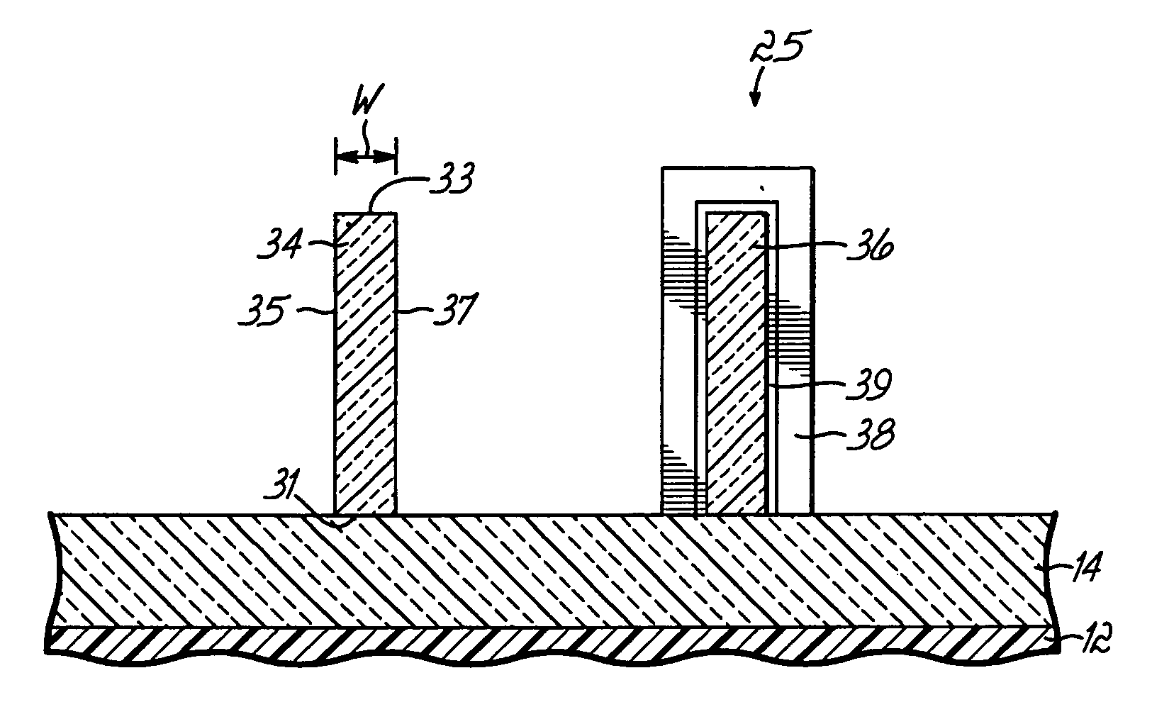
[0017] The present invention provides methods of making a semiconductor structure consisting of a monocrystalline silicon body that may be used as a fin body in a fin-type field effect transistor (FinFET), as well as semiconductor structures made by the methods. The body, which may built by the present invention on a semiconductor-on-insulator (SOI) wafer or on a bulk substrate, is formed with significantly improved shape control in comparison with conventional subtractive etching methods of making such bodies. These substantially uniform width, narrow bodies of low-defect density monocrystalline silicon are ideal for use as fin bodies in fully-depleted FinFET device structures. The present invention will now be described in greater detail by referring to the drawings that accompany the present application.

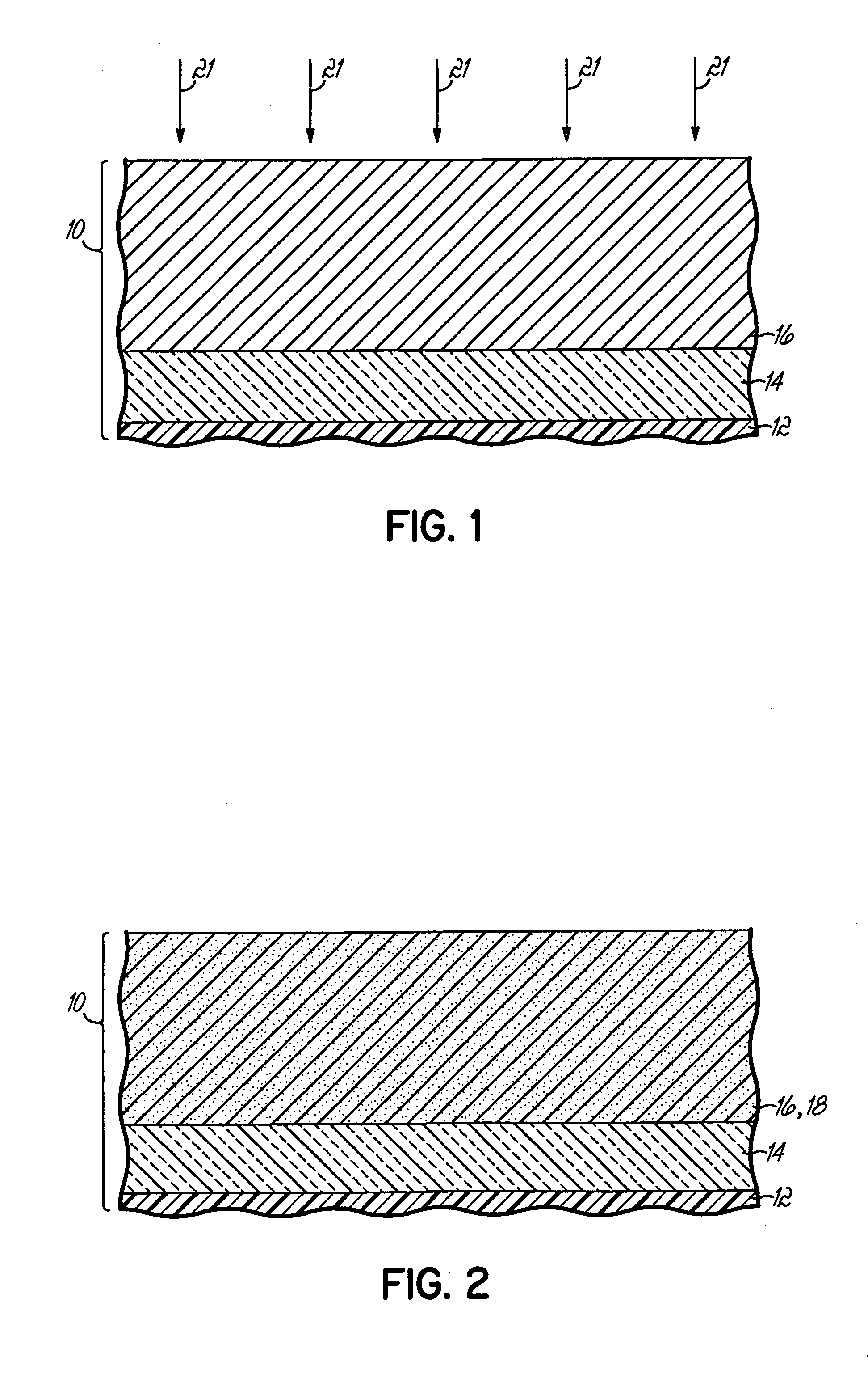
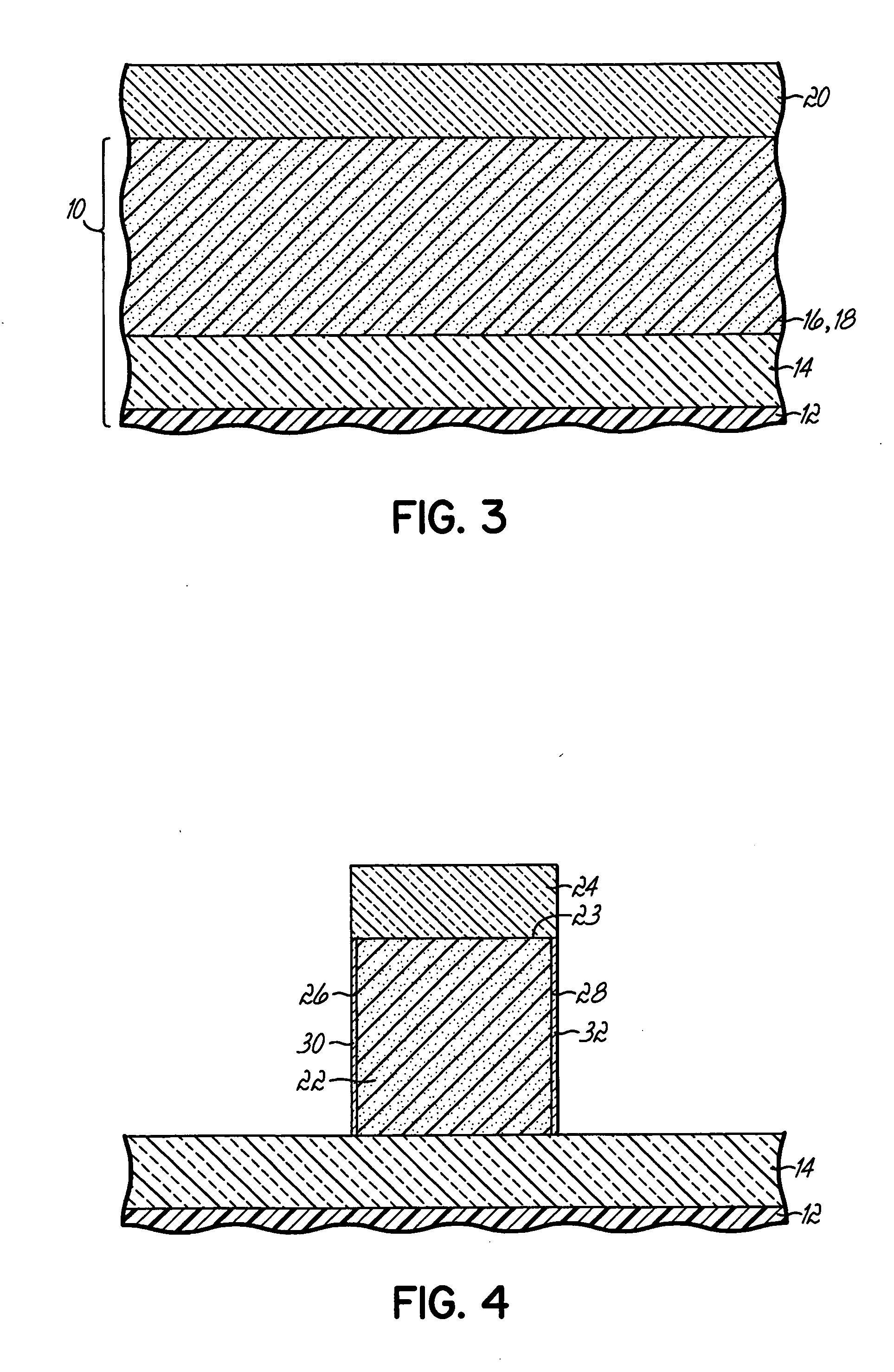
[0018] With reference to FIGS. 1 and 2 and in accordance with an embodiment of the present invention, an SOI wafer 10 comprises a semiconductor substrate 12, a buried insulator l...


PUM

PropertyMeasurementUnit
thicknessaaaaaaaaaa
thicknessaaaaaaaaaa
current densityaaaaaaaaaa

Abstract

Methods of fabricating a semiconductor structure in which a body of monocrystalline silicon is formed on a sidewall of a sacrificial mandrel and semiconductor structures made by the methods. After the body of monocrystalline silicon is formed, the sacrificial material of the mandrel is removed selective to the monocrystalline silicon of the body. The mandrel may be composed of porous silicon and the body may be fabricated using either a semiconductor-on-insulator substrate or a bulk substrate. The body may be used to fabricate a fin body of a fin-type field effect transistor.

Description

FIELD OF THE INVENTION [0001] The invention relates generally to methods for fabricating semiconductor structures and semiconductor structures and, in particular, to methods of forming a body of monocrystalline silicon using a temporary mandrel of a sacrificial material and monocrystalline silicon bodies formed by these methods. BACKGROUND OF THE INVENTION [0002] Non-planar, three-dimensional device structures are being investigated for use in integrated circuits as a replacement for planar devices, which have limitations on scalability. In particular, fin-type field effect transistors (FinFETs) are low-power, high speed non-planar devices that can be more densely packed on a substrate than traditional planar transistors. In addition, FinFETs also offer superior short channel scalability, reduced threshold voltage swing, higher mobility, and the ability to operate at lower supply voltages than traditional planar transistors. [0003] Integrated circuits that include FinFETs may be fab...

Claims


Application Information

Patent Timeline
Patent Type & Authority Applications(United States)
IPC IPC(8): H01L21/8234
CPCH01L29/66795H01L29/785
Inventor CHENG, KANGGUOMANDELMAN, JACK ALLAN
Owner GLOBALFOUNDRIES US INC
Why Eureka
Try Eureka