
Light emitting diode chip scale packaging structure

Active Publication Date: 2017-12-14
LEXTAR ELECTRONICS CORP
View PDF2 Cites 1 Cited by
  • Summary
  • Abstract
  • Description
  • Claims
  • Application Information

AI Technical Summary

Benefits of technology

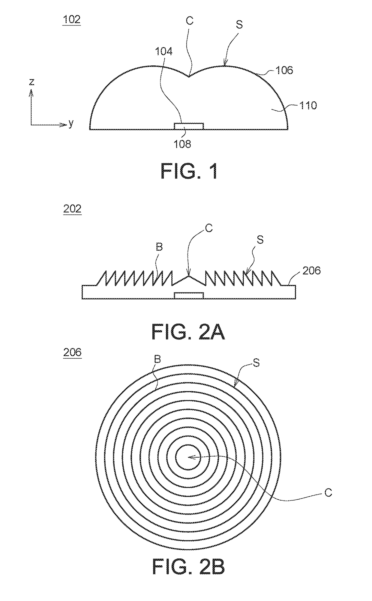
The present disclosure relates to a light emitting device that uses a lens with a specific curve to direct light emitted from the device to a specific location, resulting in improved display effect. The lens has a Fresnel lens structure, which reduces the amount of material used, manufacturing costs, weight, volume, and thickness of the device. The device has a small thickness, which facilitates miniaturizing or thinning designs. The manufacturing method allows for a larger tolerance in the device. The desired light emitting effect of the device is maintained.

Problems solved by technology

However, a manufacturing process for the device often requires a high accuracy and relates to a pack plate design for a module, with high technical difficulty.
In addition, a tolerance for an optical shift is low.
Therefore, there are the problems of risk of disposing an element and cost needed to be overcome.
However, it is very difficult to achieve a thin product when using the refractive lens with limitation of its physical threshold.
Moreover, there is an undesirable optical phenomenon resulted from a shift of disposing an element during assembling a whole module, which relates to an accuracy problem of the disposing step.

Method used


Image

  • Light emitting diode chip scale packaging structure
  • Light emitting diode chip scale packaging structure
  • Light emitting diode chip scale packaging structure

Examples


Embodiment Construction

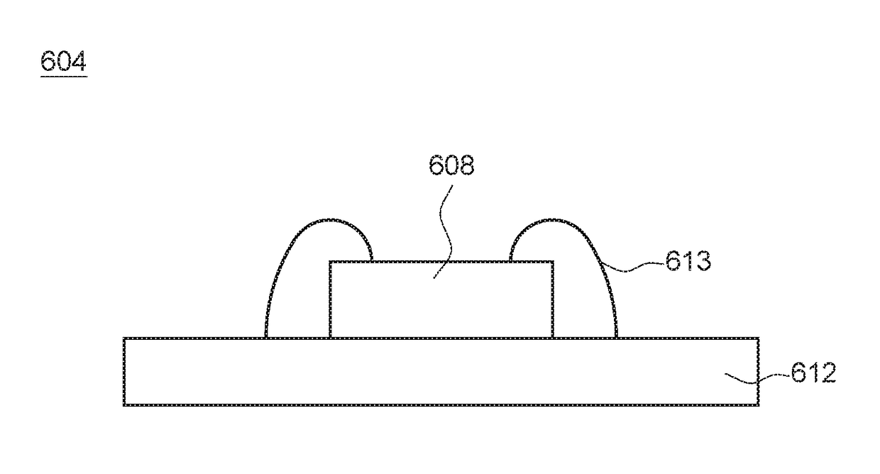
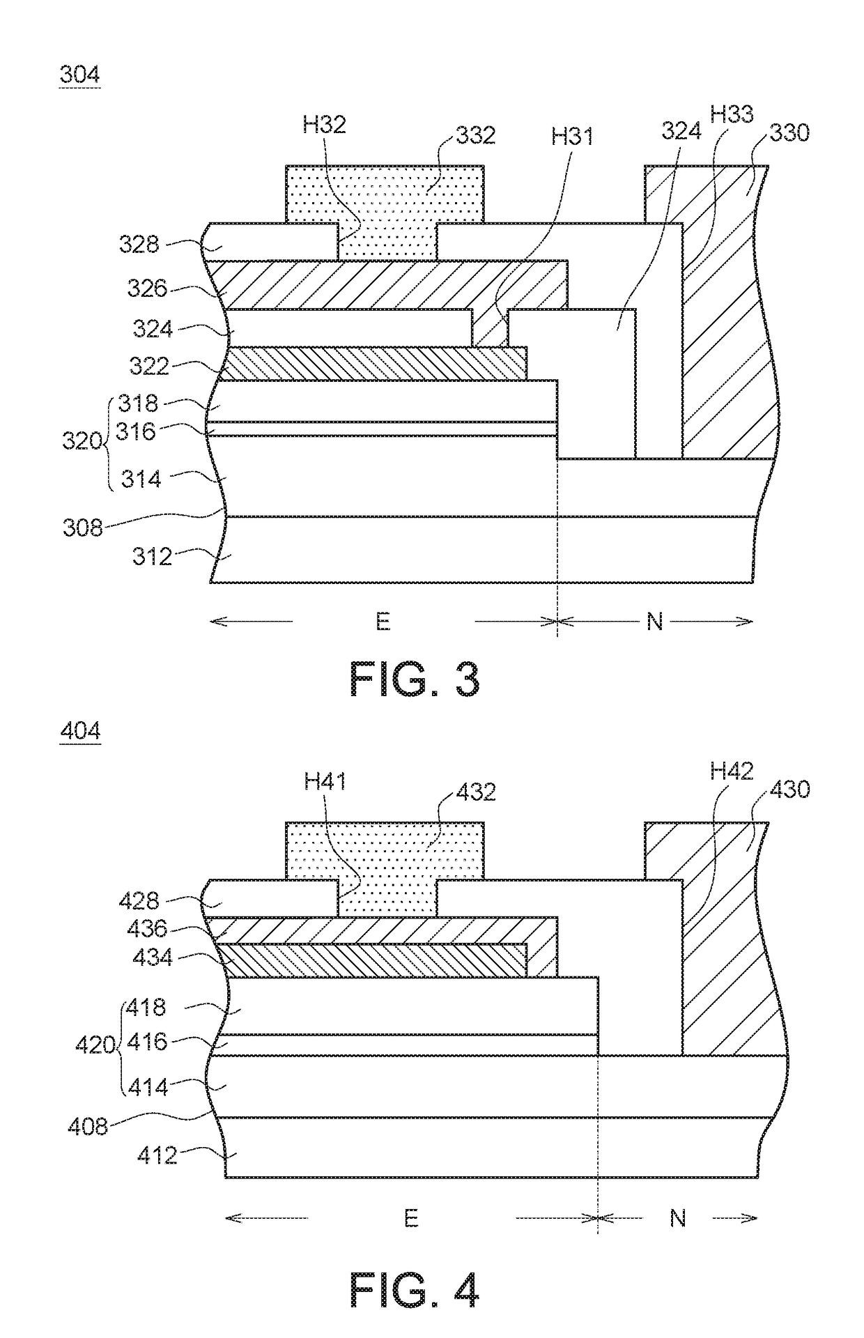
[0020]Embodiments in the present disclosure provide a light emitting diode packaging structure such as a light emitting diode chip scale packaging structure, and a light emitting device comprising the light emitting diode packaging structure, and a manufacturing method for the same. The light emitting diode packaging structure can reveal excellent luminous efficiency and display effect.

[0021]Embodiments are provided hereinafter with reference to the accompanying drawings for describing the related procedures and configurations. It is noted that not all embodiments of the invention are shown. The identical and / or similar elements of the embodiments are designated with the same and / or similar reference numerals. Also, it is noted that there may be other embodiments of the present disclosure which are not specifically illustrated. Modifications and variations can be made without departing from the spirit of the disclosure to meet the requirements of the practical applications. It is al...


PUM


Abstract

A light emitting diode chip scale packaging structure is disclosed. The light emitting diode chip scale packaging structure comprises a light emitting diode chip and a lens. The lens covers the light emitting diode chip. A curve of an outer surface of the lens in a cross-section view substantially complies with a polynomial of:z=Σi=0nai*yi,A center point of the curve corresponding to the light emitting diode chip is a zero point of y-z coordinate axes. z is a variable of vertical axis of the curve. y is a variable of horizontal axis of the curve. ai is a constant coefficient in a term of ith degree. 3<n≦6.

Description

BACKGROUND[0001]This application claims the benefit of Taiwan application Serial No. 105118389, filed Jun. 13, 2016, the subject matter of which is incorporated herein by reference.TECHNICAL FIELD[0002]The disclosure relates to a light emitting diode packaging structure, and more particularly to a light emitting diode packaging structure having a lens.DESCRIPTION OF THE RELATED ART[0003]Due to advantages of long lifetime, small volume, great resistance to vibration, low heat emission, and low power consumption, light emitting diodes (LEDs) have been extensively applied in various home appliances and instruments as indicators or light sources. With recent development towards multicolor and high illumination, the applications of the LEDs are extended to various display devices, lighting devices, etc.[0004]A displaying effect of a product would be affected by a luminescence property of a device.[0005]For example, a liquid crystal display device may use a back light module. A direct typ...

Claims


Application Information

Patent Timeline
IPC IPC(8): H01L33/20H01L33/50H01L33/52H01L33/58H01L27/15
CPCH01L33/20H01L33/58H01L33/50H01L2933/005H01L33/52H01L2933/0058H01L27/156H01L33/54H01L33/502
Inventor HUANG, CHE-HSUANCHANG, SHU-HSIUSU, HSIN-LUNLIN, CHIH-HAOTSAI, TZONG-LIANG
Owner LEXTAR ELECTRONICS CORP
Learn More