Imaging device and imaging system

Active Publication Date: 2017-12-14
CANON KK
View PDF10 Cites 21 Cited by
  • Summary
  • Abstract
  • Description
  • Claims
  • Application Information

AI Technical Summary

Benefits of technology

The invention provides an imaging device and system that can capture wide dynamic range moving images while autofocusing at high performance levels.

Problems solved by technology

The method disclosed in Japanese Patent Application Laid-Open No. 2015-201834 achieves generation of both a high dynamic range image and phase difference information, but does not necessarily achieve sufficient autofocus function.

Method used


Image

  • Imaging device and imaging system
  • Imaging device and imaging system
  • Imaging device and imaging system

Examples


first embodiment

[0031]An imaging device and a method for driving the same according to a first embodiment of the present invention will be described with reference to FIGS. 1 to 7B.

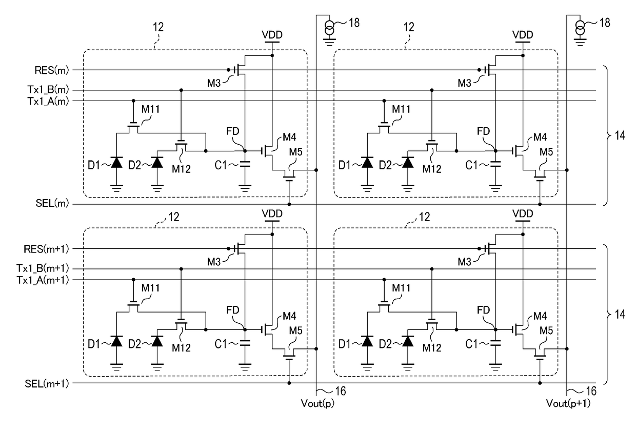
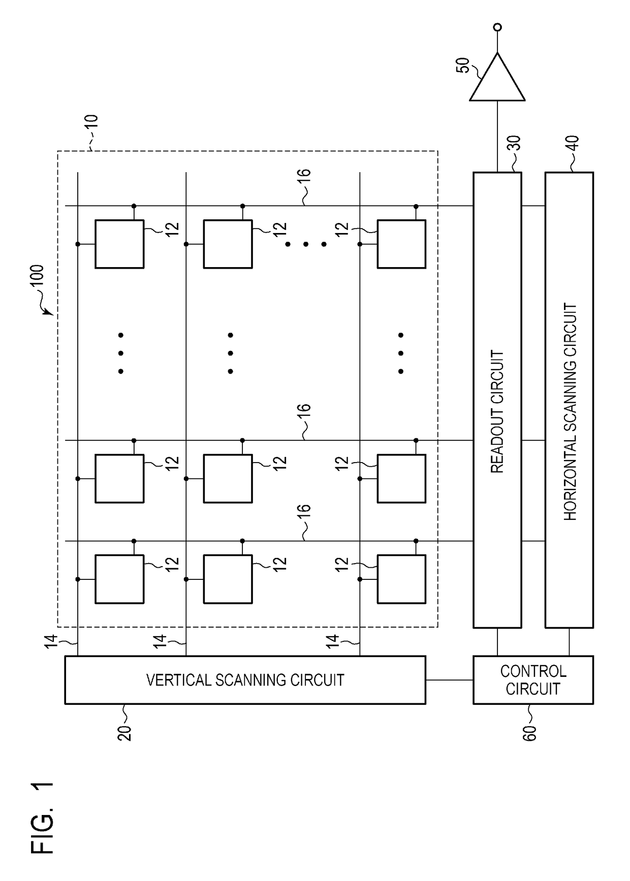
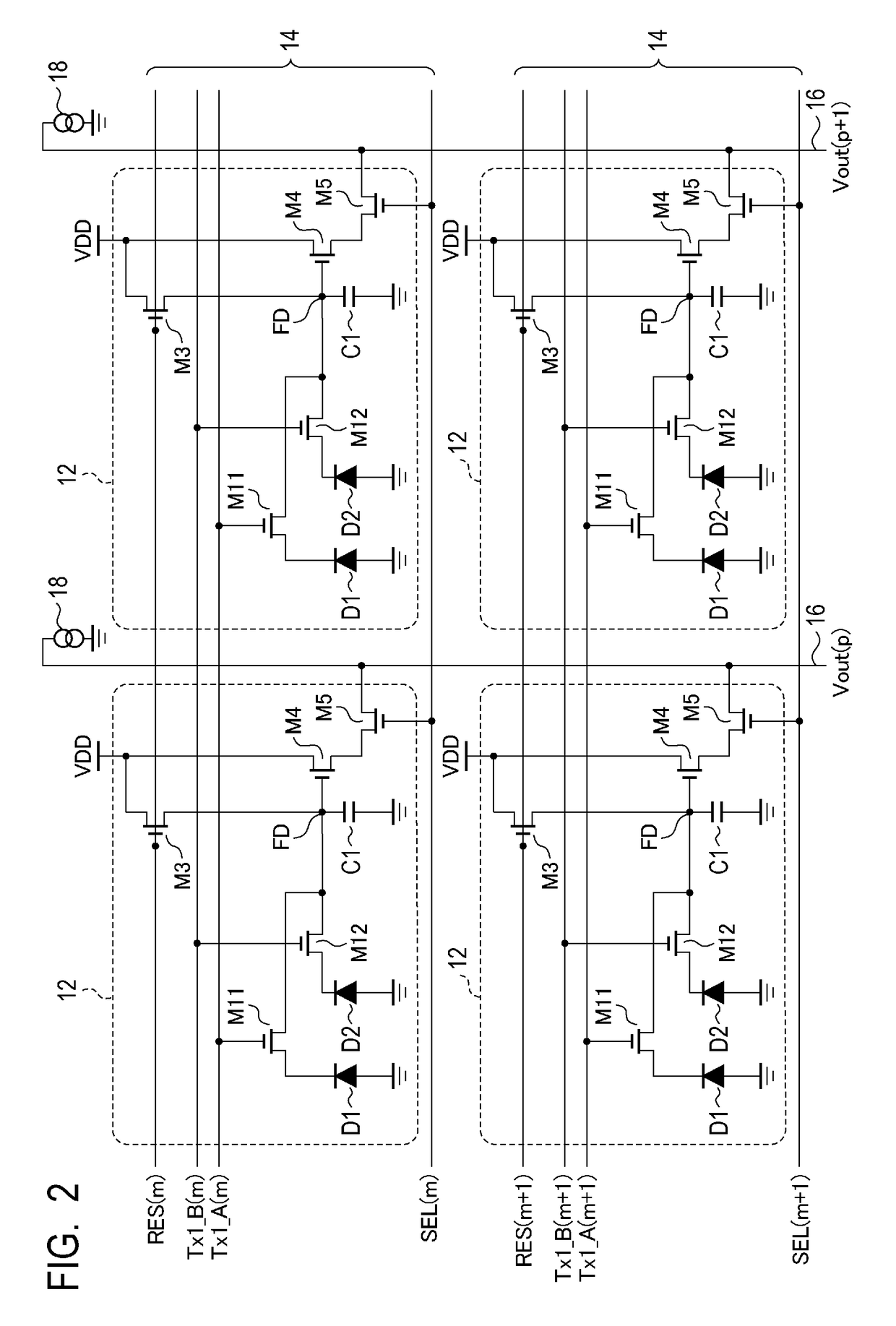
[0032]FIG. 1 is a block diagram illustrating the schematic configuration of the imaging device according to the present embodiment. FIG. 2 is a diagram illustrating an example of configuration of a pixel circuit of the imaging device according to the present embodiment. FIG. 3 is a schematic diagram illustrating an example of a plan-view layout of a pixel array unit of the imaging device according to the present embodiment. FIG. 4 is a cross-sectional view illustrating an example of a pixel structure in the imaging device according to the present embodiment. FIGS. 5A and 5B are schematic diagrams illustrating a method for driving the imaging device according to the present embodiment. FIGS. 6A to 7B are timing charts illustrating the method for driving the imaging device according to the present embodiment.

[0033]First, t...

second embodiment

[0079]An imaging device and a method for driving the same according to a second embodiment of the present invention will be described with reference to FIGS. 8 to 12. Components that are the same as those in the imaging device according to the first embodiment illustrated in FIGS. 1 to 7B are denoted by the same reference signs as those used in the first embodiment, and are either not described or described only briefly.

[0080]FIG. 8 is a diagram illustrating an example configuration of pixel circuits of the imaging device according to the present embodiment. FIG. 9 is a schematic diagram illustrating an example plan-view layout of a pixel array unit of the imaging device according to the present embodiment. FIG. 10 is a cross-sectional view illustrating an example pixel structure in the imaging device according to the present embodiment. FIG. 11 is a schematic view illustrating a method for driving the imaging device according to the present embodiment. FIG. 12 is a timing chart ill...

third embodiment

[0099]An imaging device and a method for driving the same according to a third embodiment of the present invention will be described with reference to FIGS. 13 to 16. Components that are the same as those in the imaging devices according to the first and second embodiments illustrated in FIGS. 1 to 12 are denoted by the same reference signs as those used in the first and second embodiments, and are either not described or described only briefly.

[0100]FIG. 13 is a diagram illustrating an example configuration of pixel circuits of the imaging device according to the present embodiment. FIG. 14 is a schematic diagram illustrating an example plan-view layout of a pixel array unit of the imaging device according to the present embodiment. FIG. 15 is a schematic view illustrating a method for driving the imaging device according to the present embodiment. FIG. 16 is a timing chart illustrating the method for driving the imaging device according to the present embodiment.

[0101]First, a des...


PUM


Abstract

An imaging device includes pixels each including first and second photoelectric conversion units on which pupil-divided parts of incident light are incident and a holding unit that holds charges transferred from the first and second photoelectric conversion units, and outputting signals based on amounts of charges held by the holding unit. Each pixel outputs a first signal and a second signal based on amounts of charges generated by the first photoelectric conversion unit and by the first and second photoelectric conversion units, respectively, during a first exposure time, and a third signal and a fourth signal based on amounts of charges generated by the first photoelectric conversion unit and by the first and second photoelectric conversion units, respectively, during a second exposure time. The first and second signals are output before the third and fourth signals in one frame and after the third and fourth signals in another frame.

Description

BACKGROUND OF THE INVENTIONField of the Invention[0001]The present invention relates to an imaging device and an imaging system.Description of the Related Art[0002]For an imaging device such as a CMOS image sensor, a technique has been proposed which generates an image signal of a high dynamic range by combining two image signals obtained under different imaging conditions. In a method disclosed in Japanese Patent Application Laid-Open No. 2015-201834, pixels having different sensitivities are provided, and pixel signals from these pixels are used to generate a high dynamic range image and to generate phase difference information.[0003]The method disclosed in Japanese Patent Application Laid-Open No. 2015-201834 achieves generation of both a high dynamic range image and phase difference information, but does not necessarily achieve sufficient autofocus function.SUMMARY OF THE INVENTION[0004]An object of the present invention is to provide an imaging device and an imaging system capa...

Claims


Application Information

Patent Timeline
IPC IPC(8): H04N5/355H04N5/369H04N5/378G02B7/34
CPCH04N5/35554H04N5/378G02B7/34H04N5/3696H01L27/14623H01L27/1464H01L27/14643H04N25/583H04N25/704H04N25/778H04N25/78H04N25/75
Inventor KAWABATA, KAZUNARIKOBAYASHI, MASAHIROONUKI, YUSUKE
Owner CANON KK
Why Eureka
Try Eureka