

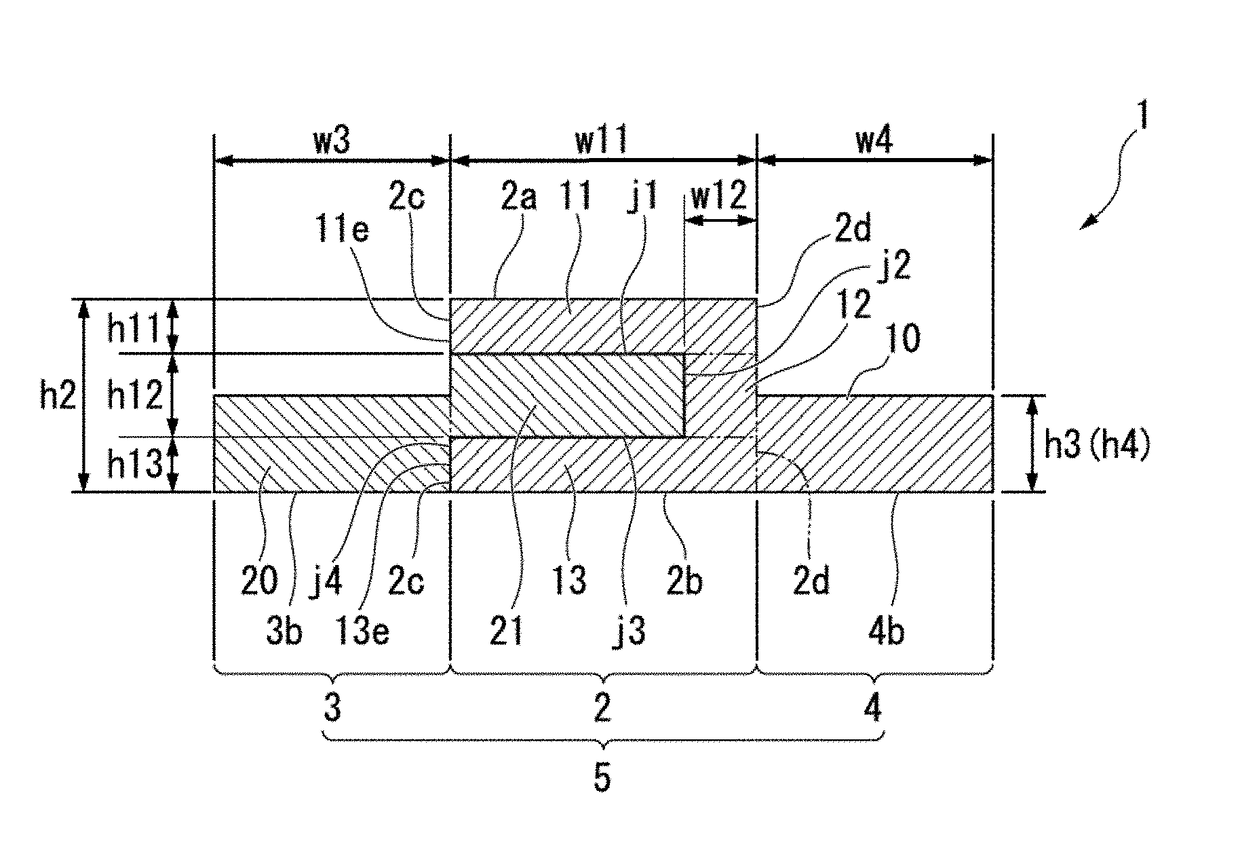
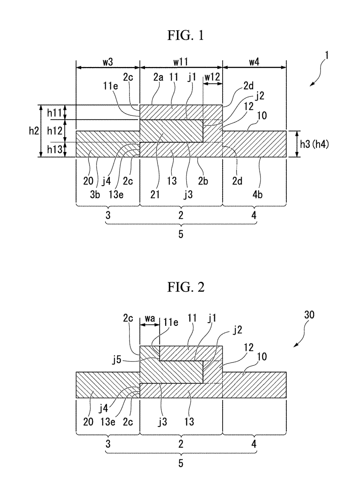
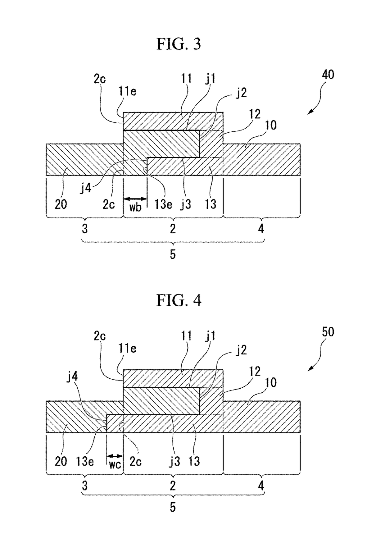
Optical modulation element, optical modulator, and manufacturing method of optical modulation element
a manufacturing method and optical modulation technology, applied in non-linear optics, instruments, optics, etc., can solve the problems of insufficient pn junction plane area for devices requiring higher modulation efficiency, and insufficient pn junction plane area for devices requiring higher modulation efficiency, and achieve the effect of higher modulation efficiency
- Summary
- Abstract
- Description
- Claims
- Application Information
AI Technical Summary
Benefits of technology
Problems solved by technology
Method used
Image

Examples
modified example
[0098]As an another example of the manufacturing method of an optical modulation element according to an embodiment, a manufacturing method of the optical modulation element 50 having the structure exemplarily shown in FIG. 4 will be explained in detail with reference to FIG. 7A-FIG. 7D.
[0099]Referring to FIG. 7A and FIG. 7B, in the same way as the above-described manufacturing method, the first slab part 3, the second slab part 4, and the rib part 2 which is covered with the first mask m1 are formed. The first conductive type dopant and the second conductive type dopant are implanted to the substrate S to form a first layer s1 of the first conductive type, a second layer s2 of the second conductive type and a third layer s3 of the first conductive type in the substrate S such that the first to third layers arranged in this order along the thickness direction of the substrate S. After that, the first mask m1 is removed.
[0100]Referring to FIG. 7C, a fourth mask m4 is formed to cover ...
examples
[0109]The modulation efficiency of the above-described optical modulation element 1 was evaluated using simulations. For comparison purposes, an optical modulation element according to a conventional example was evaluated in the same way.
[0110]Referring to FIG. 12, an optical modulation element 100 according to a conventional example has the same structure as the above-described optical modulation element 1 except for the first semiconductor region and the second semiconductor region.
[0111]A first semiconductor region 110 of the optical modulation element 100 has an upper section 111 and a lower section 113 which do not reach the first side face 2c of the rib part 2.
[0112]In the example shown in FIG. 12, the upper section 111 has substantially a rectangular shape with a width of w111 and a height of h111, while the lower section 113 has substantially a rectangular shape with a width of w111 and a height of h113. An end face 111e of the upper section 111 and an end face 113e of the l...
PUM
| Property | Measurement | Unit |
|---|---|---|
| thickness | aaaaa | aaaaa |
| conductive type | aaaaa | aaaaa |
| conductive | aaaaa | aaaaa |
Abstract
Description
Claims
Application Information