Eureka AIR delivers breakthrough ideas for toughest innovation challenges, trusted by R&D personnel around the world.

Display device and method for fabricating the same

Active Publication Date: 2018-01-25
SAMSUNG DISPLAY CO LTD
View PDF0 Cites 7 Cited by
  • Summary
  • Abstract
  • Description
  • Claims
  • Application Information

AI Technical Summary

Benefits of technology

The patent is about a display device and a method of manufacturing it that can prevent damage to the signal line when a semiconductor layer is treated with dehydrogenation. The technical effect of this invention is to improve the reliability and durability of the display device.

Problems solved by technology

However, due to a thermal treatment process during the dehydrogenation, a signal line may be damaged.

Method used


Image

  • Display device and method for fabricating the same
  • Display device and method for fabricating the same
  • Display device and method for fabricating the same

Examples


Embodiment Construction

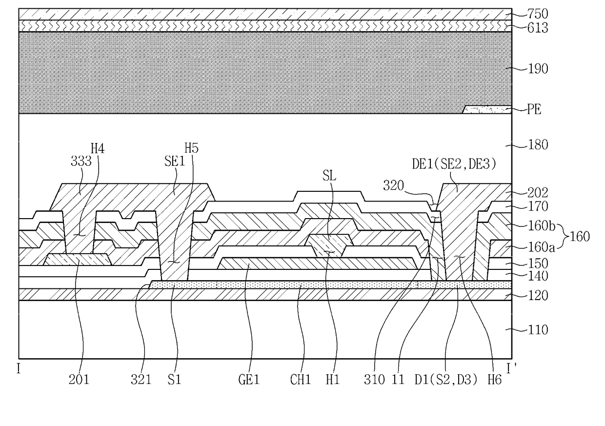
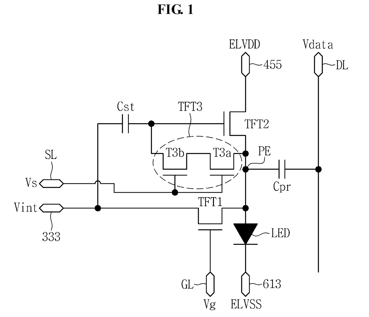
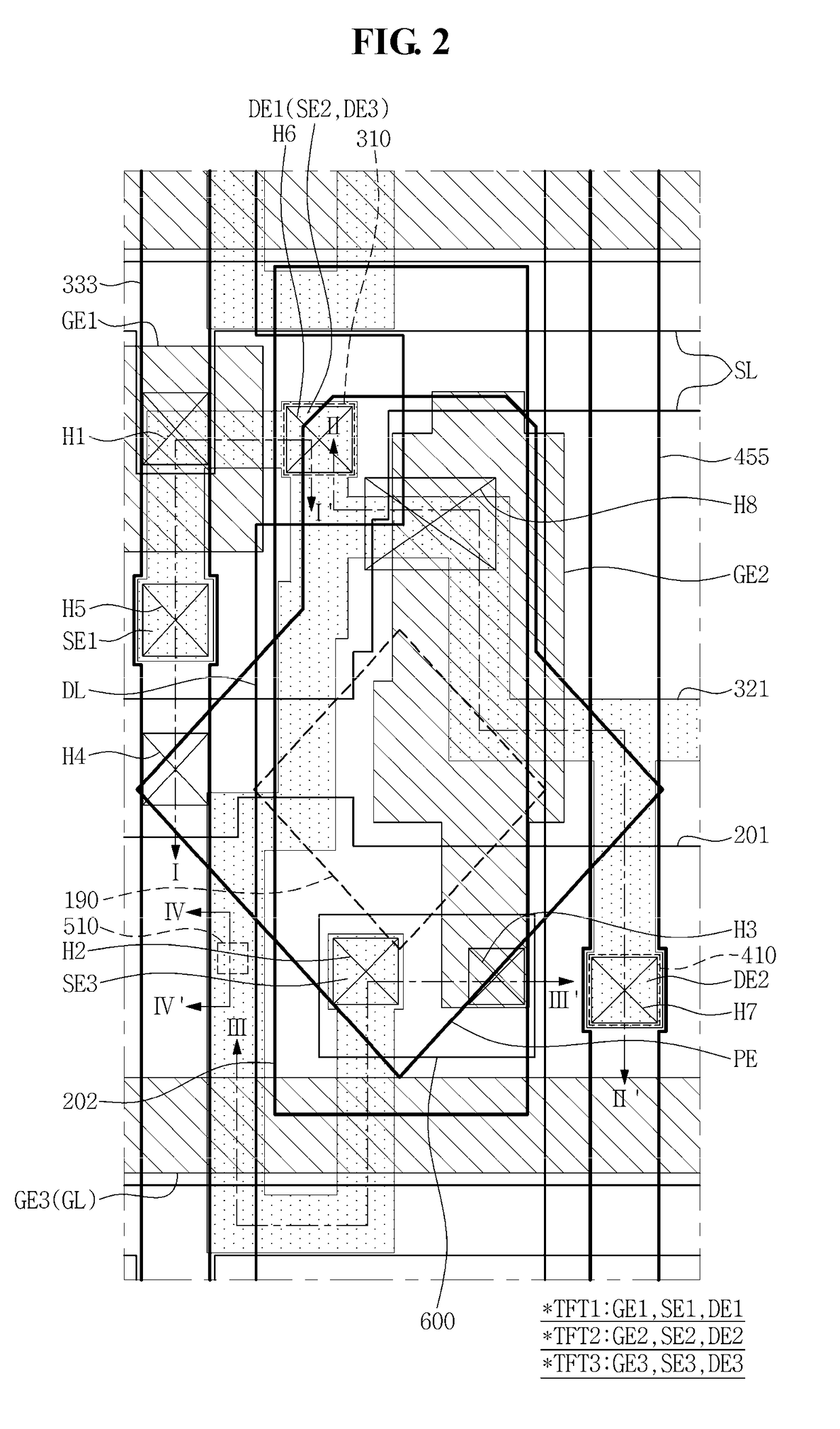
[0040]Exemplary embodiments will now be described more fully hereinafter with reference to the accompanying drawings. Although the inventive concept can be modified in various manners and have several embodiments, exemplary embodiments are illustrated in the accompanying drawings and will be mainly described in the specification. However, the scope of the inventive concept is not limited to the exemplary embodiments and should be construed as including all the changes, equivalents, and substitutions included in the spirit and scope of the inventive concept.

[0041]In the drawings, thicknesses of a plurality of layers and areas are illustrated in an enlarged manner for clarity and ease of description thereof. When a layer, area, or plate is referred to as being “on” another layer, area, or plate, it may be directly on the other layer, area, or plate, or intervening layers, areas, or plates may be present therebetween. Conversely, when a layer, area, or plate is referred to as being “di...


PUM


Abstract

A display device is capable of preventing damage to a signal line in a dehydrogenation process of a semiconductor layer and to a method of manufacturing the display device, the display device including: a substrate; at least one switching element on the substrate; a pixel electrode connected to the at least one switching element; a semiconductor layer on the substrate, the semiconductor layer providing a channel area of the at least one switching element; an insulating layer on the semiconductor layer; and a conductive layer connected to the semiconductor layer through a contact hole of the insulating layer. The insulating layer has a groove that overlaps the semiconductor layer and surrouds the conductive layer in the contact hole.

Description

CROSS-REFERENCE TO RELATED APPLICATION[0001]This application claims the priority to and all the benefits accruing under 35 U.S.C. §119 of Korean Patent Application No. 10-2016-0092562, filed on Jul. 21, 2016, with the Korean Intellectual Property Office (“KIPO”), the disclosure of which is incorporated herein in its entirety by reference.BACKGROUND1. Field[0002]Embodiments of the present inventive concept relate to a display device and a method of manufacturing the display device, and more particularly, to a display device that may effectively reduce (e.g., prevent) damage to a signal line in a dehydrogenation process of a semiconductor layer and to a method of manufacturing the display device.2. Description of the Related Art[0003]Light emitting diode (“LED”) display devices include pixels, and each pixel includes an LED and a pixel circuit for driving the LED. The pixel circuit includes a plurality of switching elements.[0004]In order to improve a threshold voltage of a switching ...

Claims


Application Information

Patent Timeline
IPC IPC(8): H01L27/32G02F1/1368G02F1/1362G02F1/1343
CPCH01L27/3223H01L27/3262H01L27/3265H01L27/3276G02F1/134309G02F1/1368G02F2201/121G02F1/136213G02F1/13439H01L2227/323G02F2201/123G02F2202/10G02F1/136286G02F1/136227G02F1/133357H10K59/123H10K59/124H10K59/1213H10K59/1201H01L27/124H10K59/1216H10K59/131H10K59/88
Inventor LEE, SUNGEUNKIM, JUNGHYUNKIM, JINTAEKAHN, KIWANYOON, JOOSUNCHOI, KWANGYOUNG
Owner SAMSUNG DISPLAY CO LTD
Why Eureka
Eureka Blog
Learn More