
Eureka
For R&D, Eureka makes reading and utilizing patents & technical documents easy.
Eureka AIR
Designed for self-driven R&D workflows. Generate viable solutions, solve complex R&D challenges, empower your innovation with AI.

Eureka Materials
Designed for material experts only. Revolutionize your material R&D, from search, analyze, to developing new materials.

TechResearch
Generate reliable direction feasibility study reports for your R&D in just a few steps.

TechSeek
Discover and master advanced knowledge NOW. Basics, ideas, possibilities, all at once.

TechMind
As an expert in R&D Theories, TechMind can generates customized viable solutions instantly.

TechRisk
Analyze your overall solution with one click, know your potential R&D risks in advance.

TechMonitor
Get weekly tech updates, stay abreast of the latest tech innovations and key insights.
Electric device and method for manufacturing electric device
- Summary
- Abstract
- Description
- Claims
- Application Information
AI Technical Summary
Benefits of technology
Problems solved by technology
Method used
Image

Examples
embodiment 1
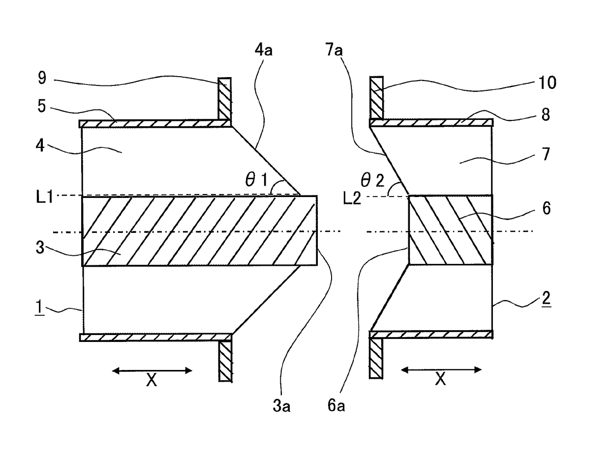
[0046]FIG. 1 is a schematic side sectional view showing an electric device according to embodiment 1 of the present invention.
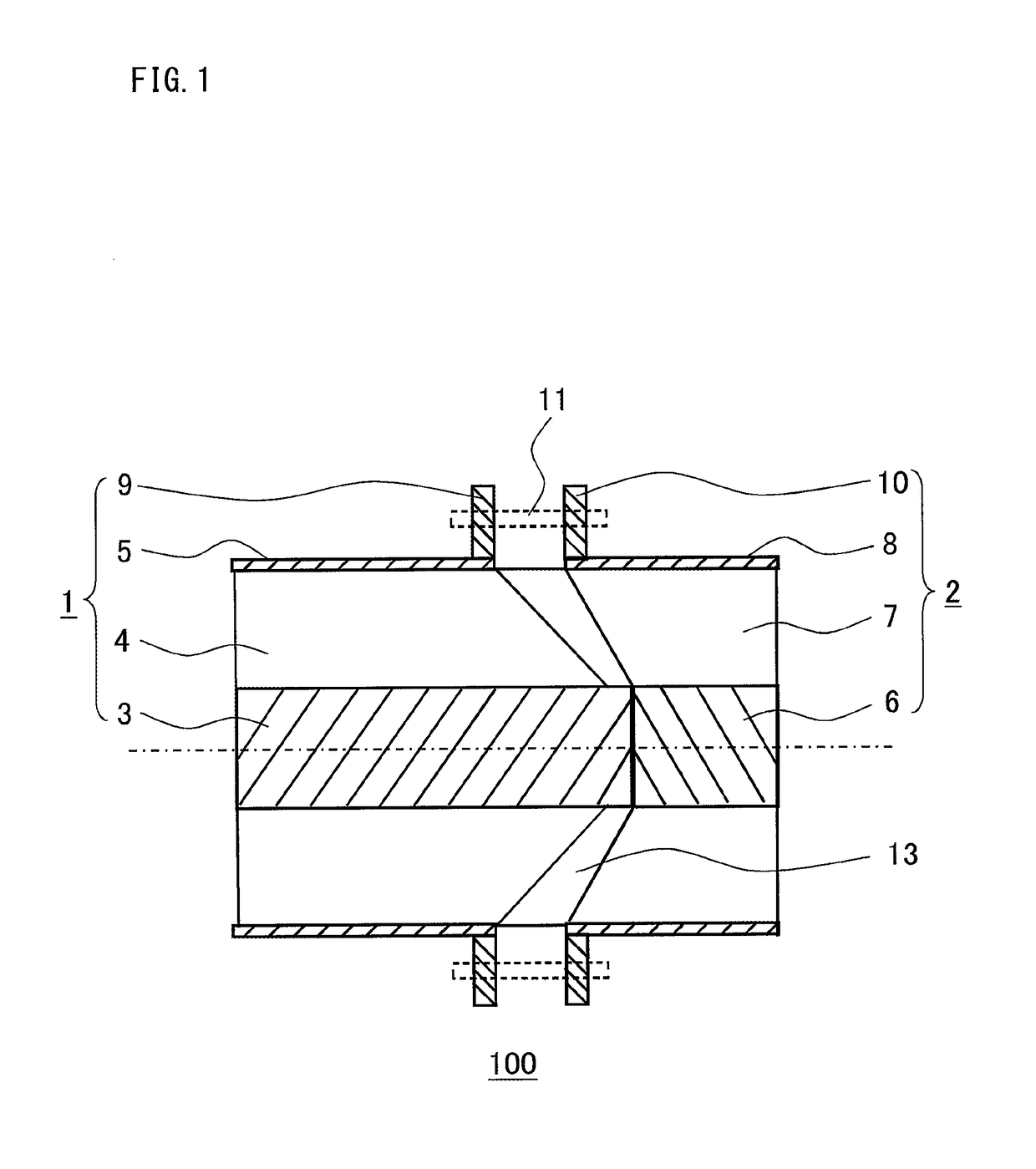
[0047]FIG. 2 is a schematic side sectional view of high-voltage devices used in the electric device according to embodiment 1 of the present invention.
[0048]FIG. 2 shows a first high-voltage device 1 and a second high-voltage device 2 composing the electric device 100 of the present embodiment before they are connected.
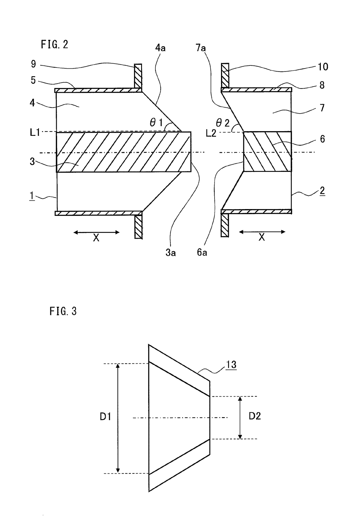
[0049]As shown in FIG. 1, in the electric device 100 of the present embodiment, the first high-voltage device 1 and the second high-voltage device 2 are connected to each other with a flexible insulating material 13 provided therebetween.
[0050]As shown in FIG. 1 and FIG. 2, the first high-voltage device 1 is composed of: a first conductor 3 which is provided at the center and to which high voltage is applied; a first solid insulating material 4 which is formed around the outer circumference of the first conductor 3 by molding and insulates the ...
embodiment 2
[0107]FIG. 6 is a schematic side sectional view of high-voltage devices used in an electric device according to embodiment 2 of the present invention.
[0108]FIG. 7 is a schematic side sectional view of a flexible insulating material used in the electric device according to embodiment 2 of the present invention.
[0109]As shown in FIG. 6, members composing the first high-voltage device 21 and the second high-voltage device 22 in the present embodiment are the same as those of the first high-voltage device 1 and the second high-voltage device 2 in embodiment 1, but the first opposing surface inclination angle θ1 of the first solid insulating material 4 is equal to the second opposing surface inclination angle θ2 of the second solid insulating material 7.
[0110]FIG. 7 shows the flexible insulating material 23 that has not yet been inserted in the electric device.
[0111]As shown in FIG. 7, the flexible insulating material 23 of the present embodiment is the same as the flexible insulating ma...
embodiment 3
[0120]FIG. 8 is a schematic side sectional view of high-voltage devices used in an electric device according to embodiment 3 of the present invention.
[0121]FIG. 9 is a schematic side sectional view of a flexible insulating material used in the electric device according to embodiment 3 of the present invention.
[0122]The electric device of the present embodiment is the same as the electric device 100 of embodiment 1 except for difference in the thickness and the elasticity modulus of the flexible insulating material.
[0123]As shown in FIG. 8, the first high-voltage device, the second high-voltage device, and the means for fastening the first high-voltage device and the second high-voltage device in the present embodiment are the same as those in embodiment 1, and the reference characters of components shown in FIG. 8 are the same as those in embodiment 1.
[0124]FIG. 9 shows a flexible insulating material 33 that has not yet been inserted in the electric device.
[0125]As shown in FIG. 9, ...
PUM
 Abstract
Description
Claims
Application Information
 - R&D Engineer
- R&D Manager
- IP Professional
- Industry Leading Data Capabilities
- Powerful AI technology
- Patent DNA Extraction
Browse by: Latest US Patents, China's latest patents, Technical Efficacy Thesaurus, Application Domain, Technology Topic, Popular Technical Reports.
© 2024 PatSnap. All rights reserved.Legal|Privacy policy|Modern Slavery Act Transparency Statement|Sitemap|About US| Contact US: help@patsnap.com