Semiconductor device, power supply circuit, and liquid crystal display device

a technology of power supply circuit and semiconductor, applied in the direction of instruments, static indicating devices, etc., can solve the problems of affecting driving capability, affecting the output voltage of the first voltage boosting circuit, and the output voltage of the second voltage boosting circuit significantly decreasing, so as to improve the ability to drive the load, reduce the influence of voltage boosting operation, and improve the effect of driving load

Active Publication Date: 2018-03-01
SEIKO EPSON CORP
View PDF8 Cites 3 Cited by
  • Summary
  • Abstract
  • Description
  • Claims
  • Application Information

AI Technical Summary

Benefits of technology

[0008]A semiconductor device according to a first aspect of the invention includes: a first regulator that stabilizes an input voltage to generate a stabilized voltage; a voltage boosting circuit that boosts the stabilized voltage to generate a boosted voltage; a second regulator that stabilizes the boosted voltage to generate a first power supply voltage; and a third regulator that is connected to the second regulator in parallel, and that stabilizes the boosted voltage to generate a second power supply voltage.
[0009]According to the first aspect of the invention, the boosted voltage that has been boosted to a sufficiently high level by the voltage boosting circuit is stabilized by the second and third regulators that are connected in parallel. Thus, even if a load current has increased, it is possible to reduce the influence thereof on the voltage boosting operation, and improve the capability to drive the load compared with known techniques. In addition, the first regulator stabilizes the input voltage supplied from a battery or the like to generate the stabilized voltage, and thereafter the voltage boosting circuit boosts the stabilized voltage to generate the boosted voltage. Accordingly, the available input voltage range can be expanded.
[0010]Here, the voltage boosting circuit may include an N-channel transistor and five P-channel transistors that are connected in series, and boost the stabilized voltage substantially three times through a charge-pump operation to generate the boosted voltage when a plurality of capacitors are connected to six terminals that are connected, in one-to-one correspondence, to the N-channel transistor and the fixe P-channel transistors. With this configuration, a boosted voltage that is about three times the stabilized voltage supplied from the first regulator can be generated with a high voltage conversion efficiency.
[0011]The first regulator may include a differential amplifier circuit that operates upon receiving a supply of the input voltage, and amplifies a difference between a reference voltage and a feedback voltage to generate the stabilized voltage, a voltage divider circuit that divides the stabilized voltage to generate the feedback voltage, and a capability selection circuit that selects a load change response capability of the first regulator by changing a value of a bias current flowing through two transistors that constitute a differential pair in the differential amplifier circuit. With this configuration, load change response capability and the power consumption of the first regulator are selected in accordance with a load state or the like, and thus unnecessary power consumption can be reduced.
[0012]Furthermore, the second or third regulator may include a differential amplifier circuit that operates upon receiving a supply of the boosted voltage, and amplifies a difference between a reference voltage and a feedback voltage to generate the first or second power supply voltage, a voltage divider circuit that divides the first or second power supply voltage to generate the feedback voltage, and a capability selection circuit that selects a load change response capability of the second or third regulator by changing a value of a bias current flowing through two transistors that constitute a differential pair in the differential amplifier circuit. With this configuration, load change response capability and the power consumption of the second or third regulator are selected in accordance with a load state or the like, and thus unnecessary power consumption can be reduced.
[0013]Otherwise, the second or third regulator may include a differential amplifier circuit that operates upon receiving a supply of the boosted voltage, and amplifies a difference between a reference voltage and a feedback voltage to generate the first or second power supply voltage, a voltage divider circuit that divides the first or second power supply voltage to generate the feedback voltage, and a voltage adjusting circuit that adjusts the first or second power supply voltage by selecting a voltage division ratio for the voltage divider circuit. With this configuration, the first or second power supply voltage is adjusted in accordance with the temperature or the like, and thus a desired power supply voltage can be generated.

Problems solved by technology

For this reason, if a load current in the first regulator increases, there is a concern that the output voltage of the first voltage boosting circuit decreases.
In this case, since the output voltage of the first voltage boosting circuit is further boosted by the second voltage boosting circuit, it is conceivable that the output voltage of the second voltage boosting circuit significantly decreases, affecting driving capability (capability to supply voltage or current) of the second regulator.

Method used


Image

  • Semiconductor device, power supply circuit, and liquid crystal display device
  • Semiconductor device, power supply circuit, and liquid crystal display device
  • Semiconductor device, power supply circuit, and liquid crystal display device

Examples


Embodiment Construction

[0026]Hereinafter, an embodiment of the invention will be described in detail with reference to the drawings. Note that like constituent elements are assigned like reference numerals to omit redundant descriptions.

[0027]Power Supply Circuit

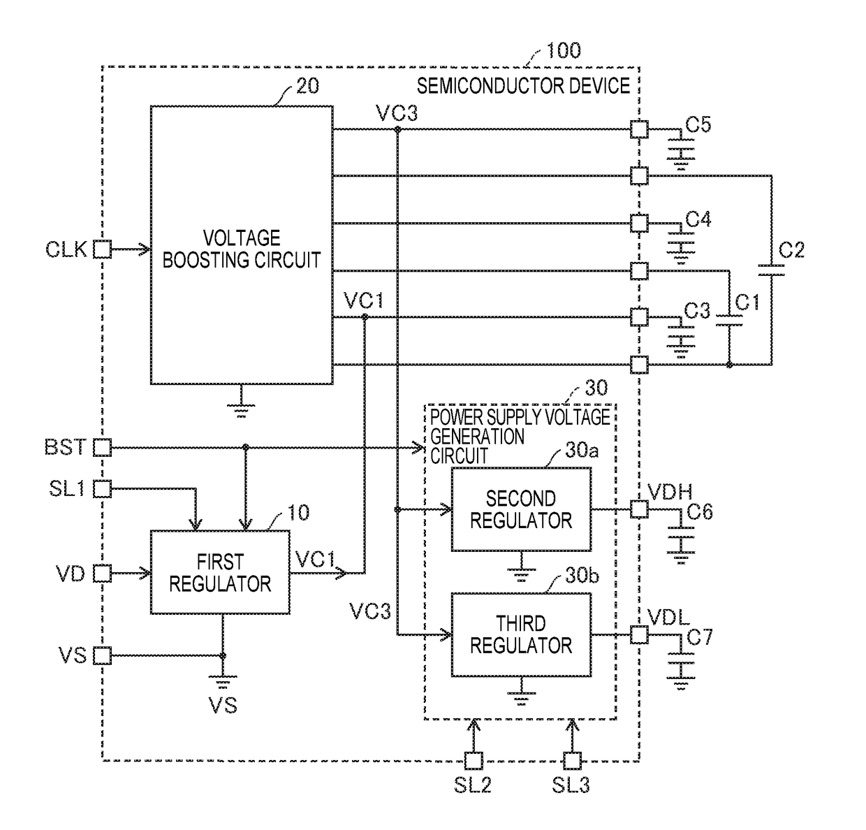
[0028]FIG. 1 is a block diagram showing an exemplary configuration of a power supply circuit according to an embodiment of the invention. As shown in FIG. 1, this power supply circuit includes a semiconductor device 100 according to an embodiment of the invention, and a plurality of external capacitors C1 to C7, which are connected to a plurality of terminals in the semiconductor device 100. The semiconductor device 100 includes a first regulator 10, a voltage boosting circuit 20, and a power supply voltage generation circuit 30. The power supply voltage generation circuit 30 includes a second regulator 30a and a third regulator 30b.

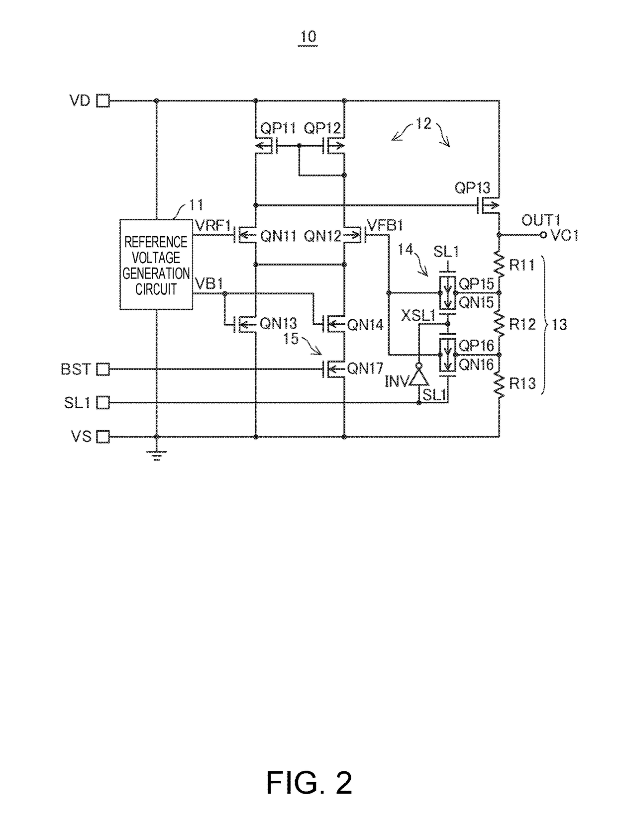
[0029]The first regulator 10 is connected to two input terminals, to which an input voltage (VD-VS) is supplied fro...


PUM


Abstract

This semiconductor device includes a first regulator that stabilizes an input voltage to generate a stabilized voltage; a voltage boosting circuit that boosts the stabilized voltage to generate a boosted voltage; a second regulator that stabilizes the boosted voltage to generate a first power supply voltage; and a third regulator that is connected to the second regulator in parallel, and that stabilizes the boosted voltage to generate a second power supply voltage.

Description

[0001]This patent application claims the benefit of Japanese Patent Application No. 2016-163443, filed on Aug. 24, 2016. The content of the aforementioned application is incorporated herein by reference in its entirety.BACKGROUND1. Technical Field[0002]The present invention relates to a semiconductor device and a power supply circuit that are used to boost an input voltage from a battery or the like to generate a desired power supply voltage. The invention also relates to a liquid crystal display device or the like that displays an image using a power supply voltage that is generated by such a semiconductor device or power supply circuit.2. Related Art[0003]For example, a liquid crystal display device requires a relatively high voltage to drive a liquid crystal panel. For this reason, in the case of portable devices such as a mobile phone or a mobile information terminal, a power supply voltage for displaying an image is generated by boosting an input voltage from a battery. For thi...

Claims


Application Information

Patent Timeline
Patent Type & Authority Applications(United States)
IPC IPC(8): G09G3/36
CPCG09G2330/02G09G3/3648G09G2310/0289G09G2330/028
Inventor ABE, SACHIYUKIOIKAWA, NOBUYUKI
Owner SEIKO EPSON CORP
Why Eureka
Try Eureka