Gate driving circuits and display devices

a driving circuit and display device technology, applied in the field of display technology, can solve the problems of mechanical and electrical reliability of the display device, higher cost, and more serious defects of high-resolution displays, so as to prevent the low-level maintaining module from causing electrical leakage and reduce the output delay of the gate strobe signal

Active Publication Date: 2018-03-01
SHENZHEN CHINA STAR OPTOELECTRONICS TECH CO LTD
View PDF0 Cites 9 Cited by
  • Summary
  • Abstract
  • Description
  • Claims
  • Application Information

AI Technical Summary

Benefits of technology

[0026]In view of the above, the gate driving circuit includes a control module for pulling down the level of the second control node to be at the low level before the gate strobe signals are outputted and during the output period of the gate cutoff signals. In this way, the third pull-down control end of the low level maintaining module is pulled down to be at the low level before the gate strobe signals are outputted and during the output period of the gate cutoff signals such that the low level maintaining module is in the off state. Thus, the low level maintaining module is prevented from causing electrical leakage so as to decrease the output delay of the gate strobe signals from the output module.

Problems solved by technology

However, such configuration not only contrary to the thin and light design, but also may cause higher cost.
When the number of pins of the peripheral driving circuits is large, the mechanical and electrical reliability of the display device may be affected.
In particular, such defect may be more serious for the high-resolution displays.
However, during the driving phase of the gate driving circuit, the level of the control pole of the low level maintaining transistor cannot be completely pulled down to be at the low level, which may result in electrical leakage.
Such defect may also increase the pull-up and pull-down delay of the output pulse of the gate driving circuit such that the efficiency of the circuit is limited.

Method used


Image

  • Gate driving circuits and display devices
  • Gate driving circuits and display devices
  • Gate driving circuits and display devices

Examples


first embodiment

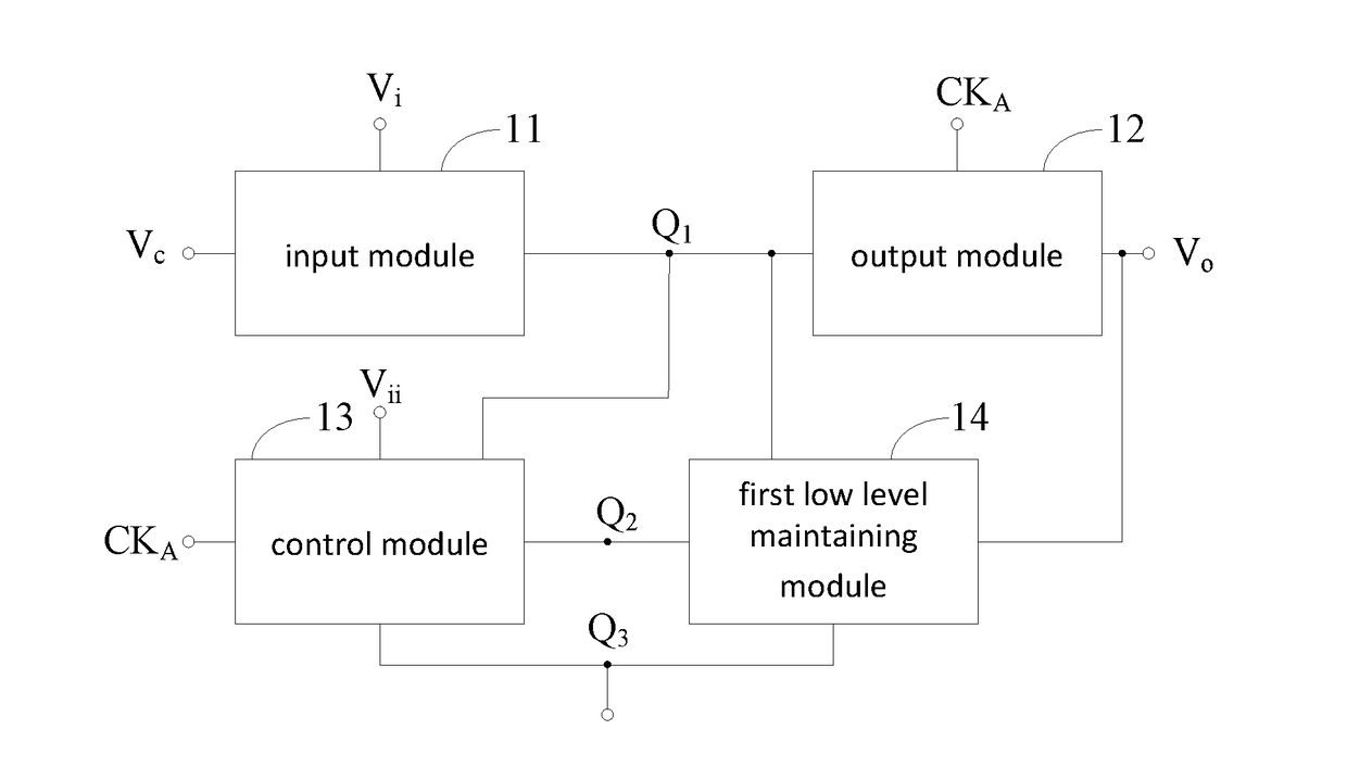
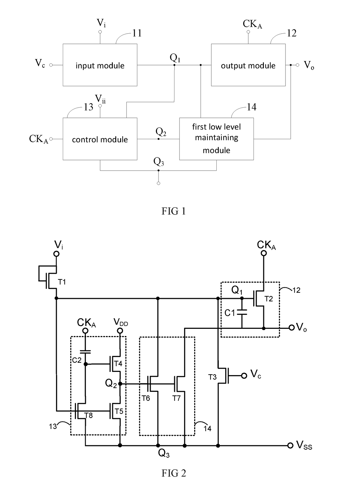
[0058]Referring to FIG. 2, the input module 11 includes a first transistor (T1) and a third transistor (T3), wherein a gate of the first transistor (T1) is short-connected with a first pole to be the pulse signals input end of the input module 11 for inputting the first pulse signals (Vi). A second pole of the first transistor (T1) and the first pole of the third transistor (T3) connect to the first control node (Q1). A second pole of the third transistor (T3) connects with the low level node (Q3). A gate of the third transistor (T3) operates as a first pull down control end of the input module 11 for inputting the first control signals (Vc).

[0059]The output module 12 includes a second transistor (T2) and a first capacitor (C1). A gate of the second transistor (T2) operates as a driving control end of the output module 12 connecting to the first control node (Q1). A first pole of the second transistor (T2) operates as the clock signal input end of the output module 12 for inputting ...

second embodiment

[0074]FIG. 5 is a circuit diagram of the gate driving unit in accordance with another embodiment. The difference between FIG. 5 and FIG. 2 resides in that, in this embodiment, the control module 13 further includes a fifteenth transistor (T15). A gate of the fifteenth transistor (T15) connects to the gate of the first transistor (T1), a first pole of the fifteenth transistor (T15) connects to the second control node (Q2), and the second pole of the fifteenth transistor (T15) connects to the low level node (Q3).

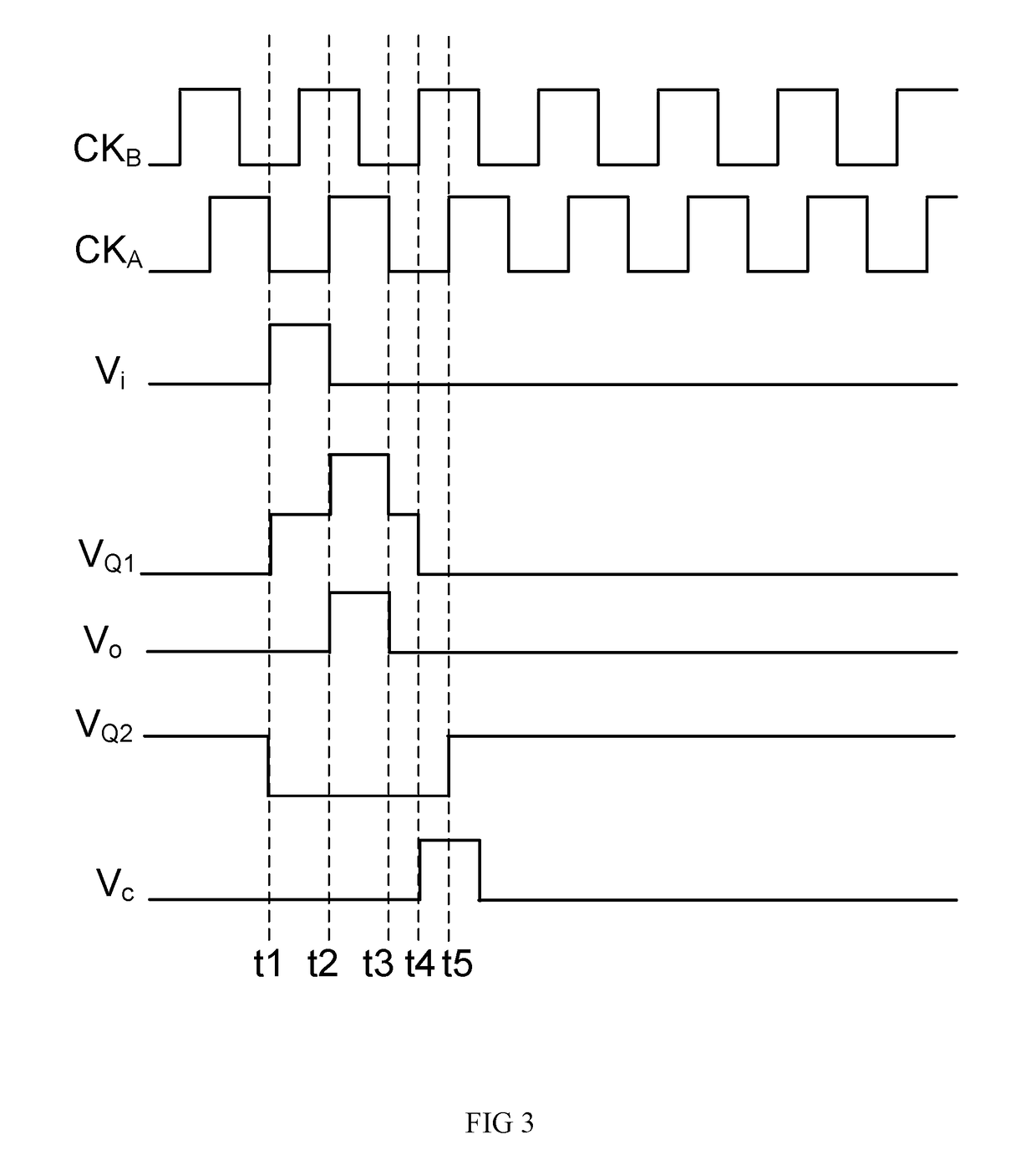
[0075]The gate of the fifteenth transistor (T15) is controlled by the first pulse signals (Vi). By configuring the fifteenth transistor (T15), at the moment t1, the fifteenth transistor (T15) is turned on by the high level control signals of the first pulse signals (Vi). In this way, the level (VQ2) of the second control node (Q2) is quickly pulled down to the low level (VL), which avoids the electrical leakage caused by the seventh transistor (T7) at the moment t1. Further, t...

third embodiment

[0077]FIG. 6 is a circuit diagram of the gate driving unit in accordance with another embodiment. The difference between FIG. 6 and FIG. 2 resides in that, in this embodiment, the control module 13 further includes a ninth transistor (T9) and a tenth transistor (T10). The gate driving unit further includes a second low level maintaining module 15, wherein the second low level maintaining module 15 includes an eleventh transistor (T11) and a twelevth transistor (T12).

[0078]Wherein a gate of the ninth transistor (T9) connects to the gate of the fourth transistor (T4), a first pole of ninth transistor (T9) is configured for inputting third clock signals (EXCK). A second pole of the ninth transistor (T9) connects with a first pole of the tenth transistor (T10), a gate of the eleventh transistor (T11), and a gate of the twelevth transistor (T12). The gate of the tenth transistor (T10) and the gate of the eighth transistor (T8) connect to the first control node (Q1), and the second pole o...


PUM


Abstract

A gate driving circuit and a display device are disclosed. The gate driving circuit includes a control module for pulling down the level of the second control node to be at the low level before the gate strobe signals are outputted and during the output period of the gate cutoff signals. In this way, the second pull-down control end of the low level maintaining module is pulled down to be at the low levels, and the low level maintaining module is in the off state. In this way, the electrical leakage of the low level maintaining module may be reduced so as to decrease the output delay of the gate signals and to enhance the efficiency of the circuit.

Description

BACKGROUND OF THE INVENTION1. Field of the Invention[0001]The present disclosure relates to display technology, and more particularly to a gate driving circuit and a display device.2. Discussion of the Related Art[0002]Flat-Panel-Displays (FPD) are characterized by attributes such as high resolution, no flicker, power-saving, and thin and light, and thus have become the main trend. Recently, FPD are designed to be high frame rate, high resolution, and narrow border.[0003]With respect to the driving method of FPDs, conventionally, an integrated circuit (IC) is adopted and the peripheral driving circuits are encapsulated on the liquid crystal panel via chip on glass (COG). However, such configuration not only contrary to the thin and light design, but also may cause higher cost. When the number of pins of the peripheral driving circuits is large, the mechanical and electrical reliability of the display device may be affected. In particular, such defect may be more serious for the high...

Claims


Application Information

Patent Timeline
Patent Type & Authority Applications(United States)
IPC IPC(8): G09G3/36
CPCG09G3/3677G09G2310/08G09G2300/0408G09G2310/0289G09G3/3674G11C19/28G09G3/3648G09G2310/0286G09G2320/0252G09G2320/0214G09G2230/00
Inventor ZHANG, SHENGDONGHU, ZHIJINLIAO, CONGWEICAO, SHIJIELEE, CHANG-YEH
Owner SHENZHEN CHINA STAR OPTOELECTRONICS TECH CO LTD
Why Eureka
Try Eureka