Cathodoluminescence-activated nanoscale imaging

a technology of cathodoluminescence and nano-scale, applied in the field of nano-scale imaging, can solve the problems of poor imaging quality, difficult to attach fluorescent labels, damage to soft materials, etc., and achieve the effect of high resolution

Active Publication Date: 2018-03-22
RGT UNIV OF CALIFORNIA
View PDF0 Cites 3 Cited by
  • Summary
  • Abstract
  • Description
  • Claims
  • Application Information

AI Technical Summary

Benefits of technology

[0006]Provided herein are cathodoluminescence-activated nanoimaging systems and methods that addresses the need in the art. The systems and methods provided can produce nanosca

Problems solved by technology

Images acquired with NSOM typically require mechanical scanning and can contain artifacts from tip-sample interactions.
Traditional electron microscopy does not use spectrally-specific excitation and can damage soft materials, such as biological samples.
Direct CL has also been used to image biological samples, but typically causes damage to the sa

Method used


Image

  • Cathodoluminescence-activated nanoscale imaging
  • Cathodoluminescence-activated nanoscale imaging
  • Cathodoluminescence-activated nanoscale imaging

Examples


embodiment 1

2. The system of embodiment 1, wherein the electron beam source is configured to contact multiple locations of the illumination layer with an electron beam without contacting the sample with the electron beam.

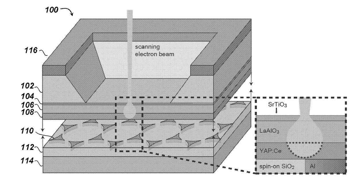
3. The system of embodiment 1, wherein the illumination layer has an optical near-field of 10 nm or less, and wherein the sample is located within the optical near-field of the illumination layer.

4. The system of any one of embodiments 1 to 3, further comprising a parabolic mirror to direct the at least a portion of the photons emitted by the illumination layer to be received by the optical detector.

5. The system of any one of embodiments 1 to 4, wherein the illumination layer comprises YAl3O and Ce3+.

embodiment 5

6. The system of embodiment 5, wherein the illumination layer is between 5 nm and 20 nm thick.

7. The system of embodiment 5, wherein the illumination layer is between 15 nm and 20 nm thick.

8. The system of any one of embodiments 1 to 7, wherein the sample comprises a biological molecule.

9. A method for imaging a sample, comprising:[0242](i) producing an electron beam from an electron beam source;[0243](ii) contacting multiple locations of an illumination layer with the electron beam,[0244]wherein the electron beam source is located above the illumination layer,[0245]wherein a sample is located below the illumination layer,[0246]wherein the contacting of the illumination layer with the electron beam excites least a portion of the illumination layer without exciting the sample, and[0247]wherein at least a portion of the excited illumination layer emits photons;[0248](iii) detecting at least a portion of the photons emitted by the excited illumination layer,[0249]wherein the detected p...

embodiment 10

11. The method of embodiment 10, wherein the illumination layer is between 5 nm and 20 nm thick.

12. The method of embodiment 10, wherein the illumination layer is between 15 nm and 20 nm thick.

13. The method of any one of embodiments 9 to 12, wherein the sample comprises a biological molecule.

14. The method of any one of embodiments 9 to 13, wherein (ii) through (iv) are repeated to produce one or more additional images of the sample sequentially over a period of time.

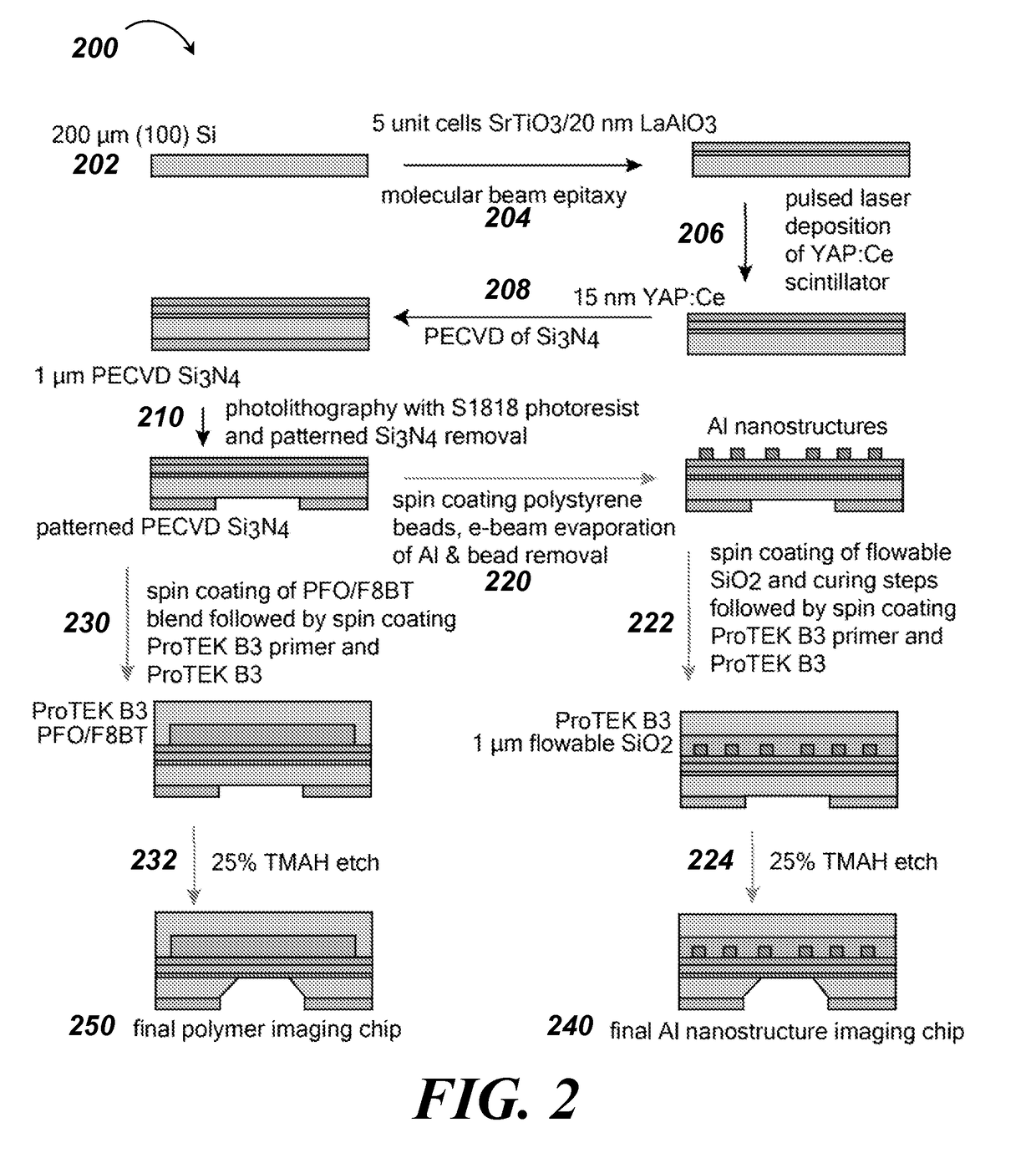
15. An imaging chip comprising:[0251]an illumination layer,[0252]wherein the illumination layer is configured to be contacted by an electron beam produced from an electron beam source positioned above the illumination layer, become excited by contact with the electron beam, and emit photons when excited;[0253]a sample layer,[0254]wherein the sample layer is configured to hold a sample and is positioned below the illumination layer;[0255]a frame layer,[0256]wherein the frame layer is configured to provide structural sup...


PUM


Abstract

Provided herein are non-invasive methods of nanoscale imaging of a sample using an illumination layer and an electron beam. For example, the electron may activate the illumination layer without activating the sample, and the illumination layer may emit cathodoluminescence to produce a nanoscale image of the sample.

Description

CROSS-REFERENCE TO RELATED APPLICATIONS[0001]This application claims priority to U.S. Provisional Patent Application No. 62 / 144,767, filed Apr. 8, 2015, which is incorporated herein by reference in its entirety.FIELD[0002]The present disclosure generally relates to nanoscale imaging, and more specifically to cathodoluminescence-activated nanoimaging of samples.BACKGROUND[0003]Near-field optical probes are valuable tools for the characterization of complex structures and processes in solid state materials, soft matter and biological samples that occur over length scales smaller than the wavelength of light. In variants of near-field scanning optical microscopy (NSOM), an optical probe is typically integrated with a scanning tip and rastered over a sample to form an image. Images acquired with NSOM typically require mechanical scanning and can contain artifacts from tip-sample interactions. Alternatively, in scanning electron microscopy (SEM), a focused electron beam is electronically...

Claims


Application Information

Patent Timeline
IPC IPC(8): G01N23/225
CPCG01N23/2254G01N23/22G01N2223/612
Inventor GINSBERG, NAOMIBISCHAK, CONNOR GREGORYHETHERINGTON, CRAIG L.KAZ, DAVID M.
Owner RGT UNIV OF CALIFORNIA
Why Eureka
Try Eureka