Display device and operating method thereof

Active Publication Date: 2018-04-26
SEMICON ENERGY LAB CO LTD
View PDF5 Cites 23 Cited by
  • Summary
  • Abstract
  • Description
  • Claims
  • Application Information

AI Technical Summary

Benefits of technology

[0019]One embodiment of the present invention can provide a novel display device. Another embodiment of the present invention can provide a display device that achieves both the detection sensitivity of a touch sensor unit and smooth input on the touch sensor unit.
[0020]Another embod

Problems solved by technology

In the case where the touch sensor unit performs detection operation at timing when the display unit rewr

Method used


Image

  • Display device and operating method thereof
  • Display device and operating method thereof
  • Display device and operating method thereof

Examples


embodiment 1

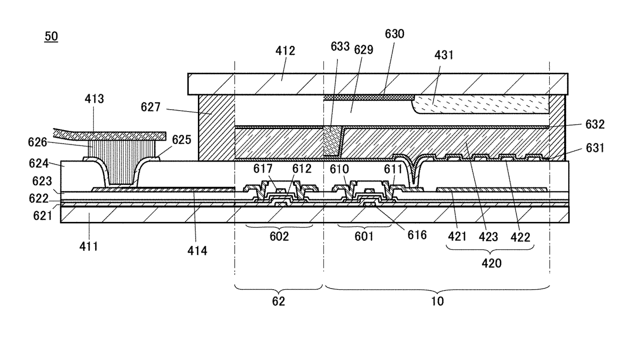
[0084]In this embodiment, a display device including a display unit and a touch sensor unit is described. In particular, the relation between image rewriting operation by the display unit and detection operation by the touch sensor unit is described.

>

[0085]FIG. 1 is a block diagram illustrating a structure example of a display device. A display device 50 includes a display unit 60, a touch sensor unit 70, and an application processor 80.

[0086]The display unit 60 includes a pixel array 61, a gate driver 62, a gate driver 63, and a source driver IC 64.

[0087]The pixel array 61 includes a plurality of pixels 10, and each pixel 10 is an active element driven by a transistor. The pixel array 61 has a function of forming a display region of the display unit 60 and displaying an image. A more specific structure example of the pixel array 61 is described later.

[0088]The gate driver 62 and the gate driver 63 have a function of driving a gate line for selecting the pixel 10. Only one of the ga...

embodiment 2

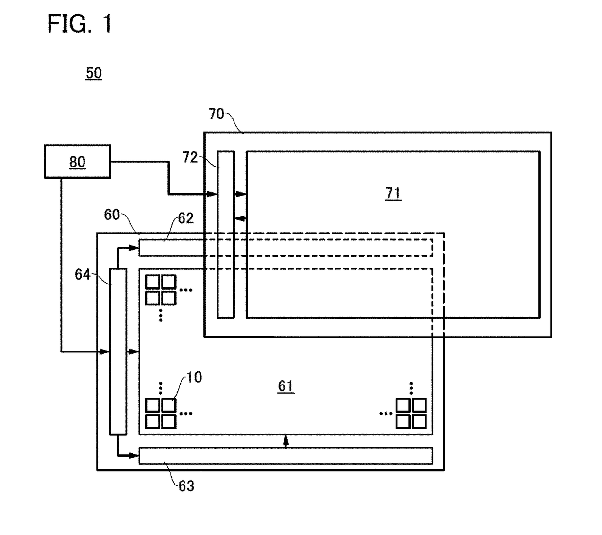
[0169]In this embodiment, a structure example of the touch sensor unit 70 mentioned in the above embodiment is described with reference to FIGS. 16A to 16C and FIGS. 17A and 17B.

[0170]A specific structure example of the touch sensor unit 70 is described with reference to FIGS. 16A to 16C and FIGS. 17A and 17B.

[0171]FIG. 16A is a top view of the touch sensor unit 70. FIGS. 16B and 16C are each a projection view illustrating part of FIG. 16A.

[0172]FIG. 17A is a top view of a portion in which a control line and a sensing signal line are adjacent to each other. FIG. 17B is a projection view that schematically illustrates an electric field generated in the adjoining portion.

[0173]The touch sensor unit 70 includes the sensor array 71. The sensor array 71 includes a wiring CL(g), a wiring ML(h), and a conductive film (see FIG. 16A). Note that g and h are each an integer of 2 or more.

[0174]For example, a conductive film divided into a plurality of regions can be used for the sensor array 71...

embodiment 3

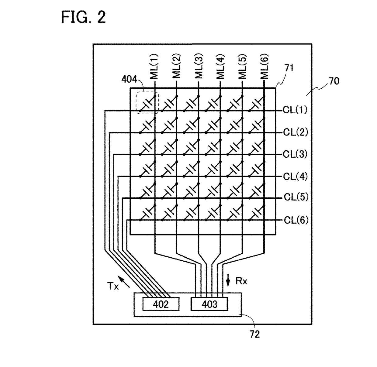
[0189]In this embodiment, a circuit configuration example of the pixel 10 described in the above embodiment is described with reference to FIG. 19, FIG. 20, and FIGS. 21A and 21B.

10a>

[0190]FIG. 19 illustrates an example of a pixel circuit that can be used for a panel including a liquid crystal element. A pixel 10a illustrated in FIG. 19 includes a transistor 301, a capacitor 303, and a liquid crystal element 304 functioning as a display element.

[0191]A gate (first gate) of the transistor 301 is electrically connected to the gate line GL, a back gate (second gate) of the transistor 301 is electrically connected to the gate, a first terminal of the transistor 301 is electrically connected to the source line SL, and a second terminal of the transistor 301 is electrically connected to a first terminal of the capacitor 303 and a first terminal of the liquid crystal element 304. A node of the second terminal of the transistor 301, the first terminal of the capacitor 303, and the first ...


PUM


Abstract

A display device that achieves both high detection sensitivity of the touch sensor unit and smooth input on the touch sensor unit is provided. A method for driving a display device includes a first period and a second period. The display device includes pixels, a gate driver, and a touch sensor unit. The touch sensor unit detects a touch in the first period and stops detecting a touch in the second period. The gate driver supplies signals to some of the pixels and does not supply signals to the other pixels in the second period.

Description

TECHNICAL FIELD[0001]One embodiment of the present invention relates to a display device and a method for operating the display device. Furthermore, one embodiment of the present invention relates to a semiconductor device.[0002]Note that one embodiment of the present invention is not limited to the above technical field. The technical field of the invention disclosed in this specification and the like relates to an object, a method, or a manufacturing method. Furthermore, one embodiment of the present invention relates to a process, a machine, manufacture, or a composition of matter.[0003]Specifically, examples of the technical field of one embodiment of the present invention disclosed in this specification and the like include a display device, a semiconductor device, an electronic device, a method for driving any of them, and a method for manufacturing any of them. In this specification and the like, a semiconductor device generally means a device that can function by utilizing s...

Claims


Application Information

Patent Timeline
IPC IPC(8): G06F3/041G06F3/044G09G3/36G09G3/3266G09G3/3225
CPCG06F3/0418G06F3/044G09G3/3677G09G3/3266G09G3/3225G02F1/13338H01L27/323H01L27/1225H01L29/7869H01L27/3232H01L27/3262G02F1/1368G02F1/13439G02F1/133553G02F2001/133565G02F2201/44G09G2300/0426G09G2310/0286G09G2330/023G02F1/136286G06F3/0412G09G3/3291G09G3/3688G09G2300/046G09G2310/04G09G2330/12G09G2360/18G09G2380/14G06F3/04166G06F3/0446G06F3/0443G06F3/0445G06F3/04182G09G3/2029G09G3/2033G09G3/2037G09G3/204H10K59/50H10K59/1213G02F1/133565H10K59/40
Inventor TAKAHASHI, KEIYAMAZAKI, SHUNPEI
Owner SEMICON ENERGY LAB CO LTD
Why Eureka
Try Eureka