Photoelectric device and image sensor and electronic device

a photoelectric device and image sensor technology, applied in the direction of semiconductor devices, solid-state devices, photovoltaic energy generation, etc., can solve the problems of deterioration of sensitivity of silicon photodiodes, low photoelectronic conversion performance, and low photoelectronic conversion efficiency of silicon-based photoelectric devices, so as to increase light absorption characteristics and wavelength selectivity

Active Publication Date: 2018-04-26
SAMSUNG ELECTRONICS CO LTD
View PDF0 Cites 3 Cited by
  • Summary
  • Abstract
  • Description
  • Claims
  • Application Information

AI Technical Summary

Benefits of technology

[0027]A photoelectric device according to example embodiments is capable of increasing light absorption characteristics and wavelength selectivity.

Problems solved by technology

In some cases, a silicon photodiode exhibits a problem of deteriorated sensitivity because of a relatively small absorption area due to relatively small pixels.
Thus, an organic photoelectric device that includes the organic material may exhibit a relatively low photoelectronic conversion efficiency, and thus relatively low photoelectronic conversion performance, relative to a silicon-based photoelectric device.

Method used


Image

  • Photoelectric device and image sensor and electronic device
  • Photoelectric device and image sensor and electronic device
  • Photoelectric device and image sensor and electronic device

Examples


example 1

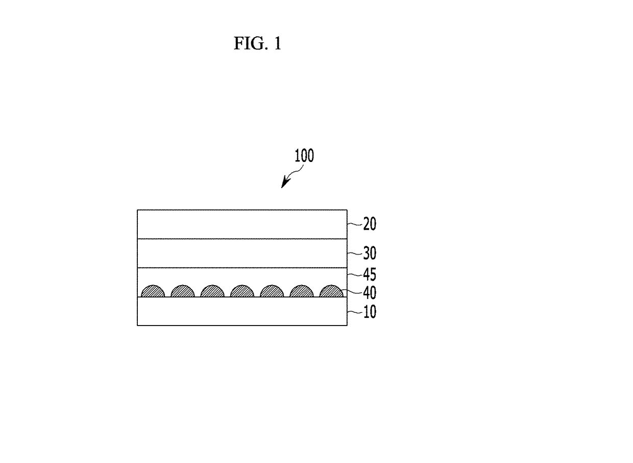
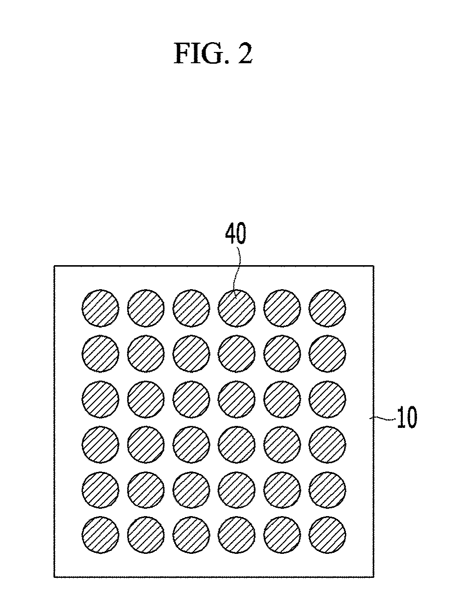
[0162]A 150 nm-thick anode is formed by sputtering ITO on a glass substrate. Subsequently, an about 2 nm-thick silver (Ag) thin film is thermally vacuum-deposited on the anode and then, heat-treated at about 150° C. to form a plurality of hemispherical silver (Ag) nanostructures having a radius of about 2 nm. On the plurality of silver (Ag) nanostructures, a compound represented by Chemical Formula A is deposited to form a 5 nm-thick auxiliary layer. On the auxiliary layer, a compound represented by Chemical Formula B as a p-type semiconductor and C60 as an n-type semiconductor are co-deposited in a volume ratio of 2:1 to form a 60 nm-thick photoelectric conversion layer. On the photoelectric conversion layer, a 7 nm-thick cathode is formed by sputtering ITO. Subsequently, a 50 nm-thick anti-reflection layer is formed by depositing aluminum oxide (Al2O3) on the cathode, and then, a glass plate is used for sealing to manufacture a photoelectric device.

example 2

[0163]A photoelectric device is manufactured according to the same method as Example 1 except for forming gold (Au) nanostructures instead of the silver (Ag) nanostructures.


PUM


Abstract

A photoelectric device includes a first electrode and a second electrode facing each other, a photoelectric conversion layer between the first electrode and the second electrode and including a light absorbing material configured to selectively absorb first visible light including one of visible light in a blue wavelength region of greater than or equal to about 380 nm and less than about 500 nm, visible light in a green wavelength region of about 500 nm to about 600 nm, and visible light in a red wavelength region of greater than about 600 nm and less than or equal to about 700 nm, and a plurality of nanostructures between the first electrode and the photoelectric conversion layer and configured to selectively reflect the first visible light.

Description

CROSS REFERENCE TO RELATED APPLICATIONS[0001]This application claims priority to and the benefit of Korean Patent Application No. 10-2016-0138671 filed in the Korean Intellectual Property Office on Oct. 24, 2016, the entire contents of which are incorporated herein by reference.BACKGROUND1. Field[0002]Example embodiments provide a photoelectric device, an image sensor, and an electronic device including the same.2. Description of the Related Art[0003]A photoelectric device may convert light into an electrical signal using photoelectric effects. A photoelectronic device may include a photodiode, a phototransistor, etc. A photoelectronic device may be applied (e.g., included in) various devices, including image sensors, a solar cell, an organic light emitting diode, some combination thereof, etc.[0004]An image sensor including a photodiode requires relatively high resolution and thus a smaller pixel. At present, a silicon photodiode is widely used. In some cases, a silicon photodiode ...

Claims


Application Information

Patent Timeline
Patent Type & Authority Applications(United States)
IPC IPC(8): H01L27/30H01L51/00
CPCH01L27/307H01L51/0046H01L51/0047H01L51/0072H01L51/0058H01L51/0053H01L51/0061H01L51/4253H01L51/447H01L51/0062H01L51/006Y02E10/549H10K39/32H10K59/32H10K59/35H10K59/38H10K85/211H10K85/649H10K85/636H10K85/626H10K85/633H10K30/30H10K85/6572H10K2102/103H01L27/14625H01L27/14629H01L27/14623H01L27/14685H01L27/14665H01L27/14643H10K71/30
Inventor YUN, SUNG YOUNGLEE, GAE HWANGPARK, KYUNG BAELEE, KWANG HEELEEM, DONG-SEOKBULLIARD, XAVIERJIN, YONG WAN
Owner SAMSUNG ELECTRONICS CO LTD
Why Eureka
Try Eureka