Method And Apparatus For Locking WDM Transmitter Carriers To A Defined Grid

a technology of frequency locking and transmitter carriers, applied in the field of method and apparatus frequency locking in wavelength division multiplexing, can solve the problems of difficult construction of absolute wavelength references on the chip, fabrication errors in interferometer or resonant filter fabricated on such a photonic chip, e.g., silicon, and achieve the effect of fast lock and easy calibration

Active Publication Date: 2018-04-26
ALCATEL-LUCENT USA INC
View PDF6 Cites 43 Cited by
  • Summary
  • Abstract
  • Description
  • Claims
  • Application Information

AI Technical Summary

Benefits of technology

[0009]We have recognized that the locking of optical carriers to a frequency set, e.g., to a grid, for use in WDM and DWDM networks can be achieved, in accordance with the principles of the disclosure, by employing at least one athermal optical filter which exhibits athermal behavior in a desired, i.e., target, frequency range to achieve a multi-frequency optical transmitter where all such frequencies are locked to a prescribed grid, e.g., the ITU grid. The athermal optical filter may be integrated on a silicon photonic integrated circuit and be relatively immune to fabrication errors. Advantageously, the need for a Fabry Perot etalon either on or off of the photonic integrated circuit is eliminated.
[0011]In one embodiment of the invention, each channel may have impressed thereon a dither signal that is detectable. The dither signal may be detected by converting the optical signal to the electrical domain, e.g., using one or more photodiodes. The magnitude of the dither signal may be detected in a conventional manner, e.g., by direct measurement or using a fast Fourier transform (FFT). In embodiments of the invention in which a unique dither signal is impressed on each channel, the individual dither signals allow for the identification of each channel, e.g., using an FFT, which is useful when multiple ones of the channels are multiplexed together. The dither signal may be impressed by either varying the intensity of the carrier produced by the individual lasers or by individually varying each respective lasing frequency of the carrier produced by the individual lasers, e.g., the carrier frequency.
[0014]A transmitter configured in accordance with the principles of the disclosure has the advantages of: 1) being integrable on a chip and therefore compact, 2) being easy to calibrate, 3) being faster to lock than systems employing prior art methods because it does not rely on accurate temperature measurements and adjustment of the whole transmitter chip, which takes a relatively long time, and 4) does not require sensitive mechanical preparation, e.g., polishing, angle alignment, etc., as is required when using an etalon.

Problems solved by technology

However, the construction of absolute wavelength references on a chip is challenging because of the large thermo-optic coefficient of both III-V and Si materials, and thus doing so requires employing advanced temperature stabilization techniques, which is undesirable.
Integration of the conventional quartz glass made Fabry-Perot etalon on a chip is also not attractive because of the relatively large dimensions of the etalon.
Moreover, any interferometer or resonant filter fabricated on such a photonic chip, e.g., one made of silicon, will suffer from fabrication errors in that it has been found that most of the time the resulting actually fabricated filter shape is significantly different from the one anticipated in the design process.
One disadvantage of such a solution is that the devices are biased with a large DC power to allow adjustment in both the negative and positive directions depending on whether the temperature of the chip increases or decreases.
This solution controls the whole transmitter chip and does not correct temperature gradients on the chip.
It also suffers from relatively large delay times because of the large dimension of the chip.
This solution, even though practical and reliable, is disadvantageous in that 1) it is not compact and cost effective, 2) it is sensitive to mechanical vibrations, and 3) it still requires active control of the temperature.

Method used


Image

  • Method And Apparatus For Locking WDM Transmitter Carriers To A Defined Grid
  • Method And Apparatus For Locking WDM Transmitter Carriers To A Defined Grid
  • Method And Apparatus For Locking WDM Transmitter Carriers To A Defined Grid

Examples


Embodiment Construction

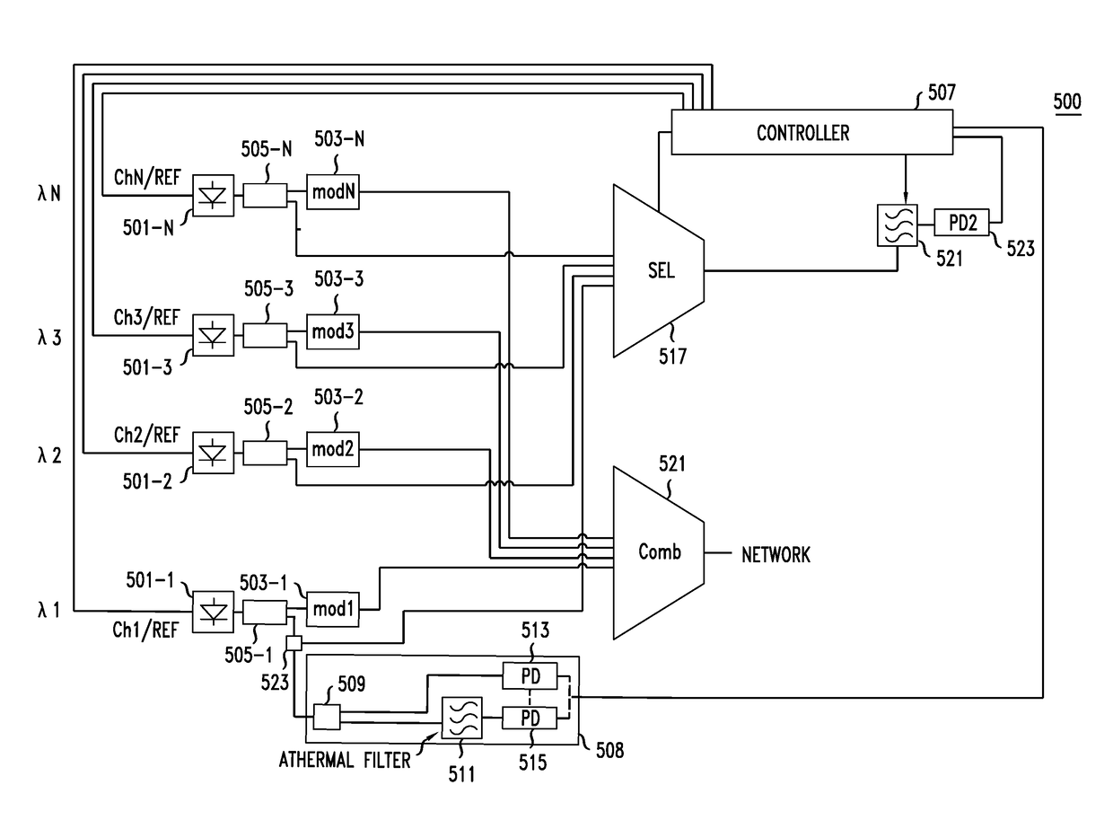
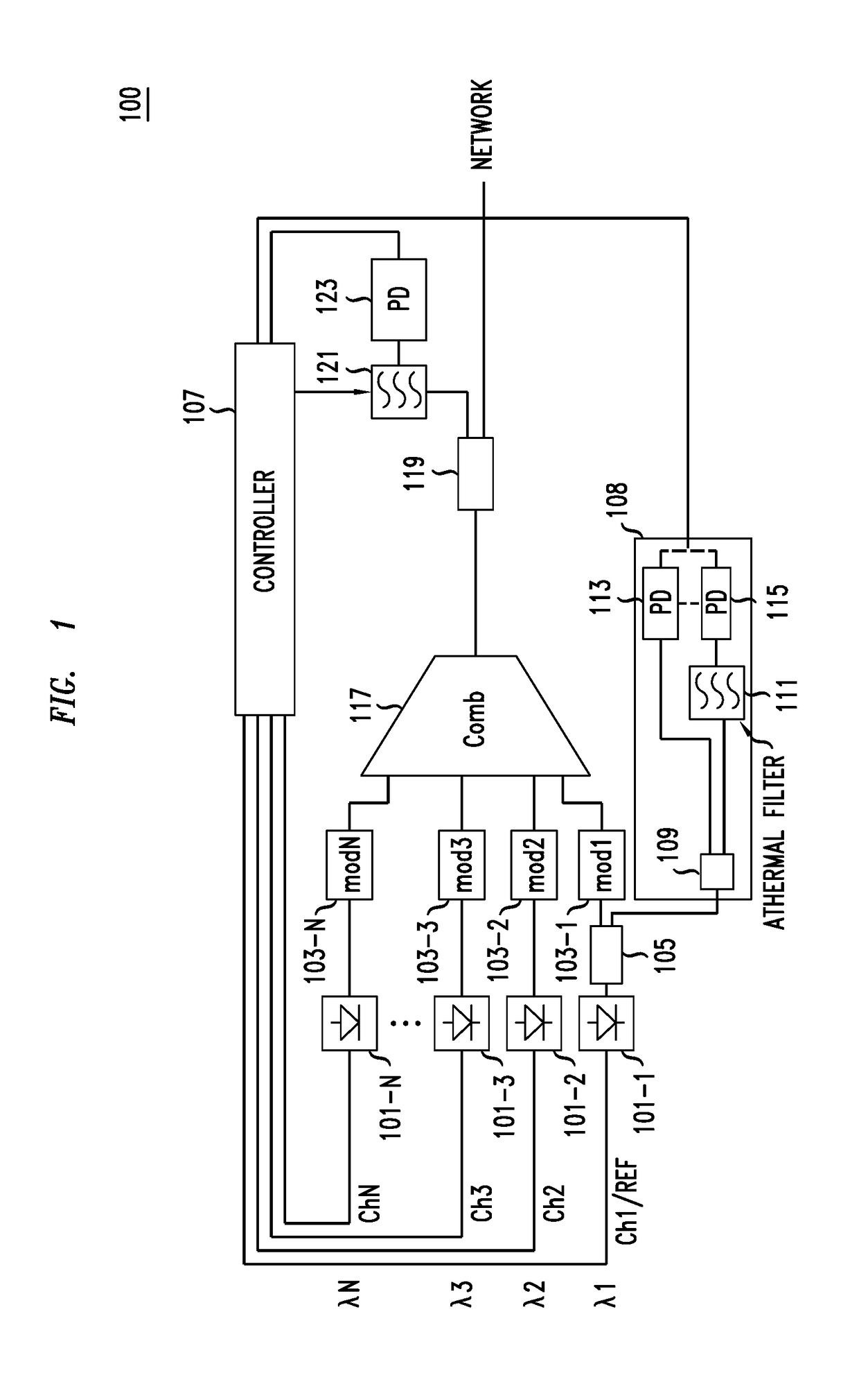
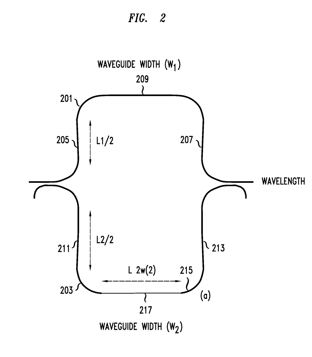
[0022]The following merely illustrates the principles of the disclosure. It will thus be appreciated that those skilled in the art will be able to devise various arrangements that, although not explicitly described or shown herein, embody the principles of the disclosure and are included within its spirit and scope. Furthermore, all examples and conditional language recited herein are principally intended expressly to be only for pedagogical purposes to aid the reader in understanding the principles of the disclosure and the concepts contributed by the inventor(s) to furthering the art, and are to be construed as being without limitation to such specifically recited examples and conditions. Moreover, all statements herein reciting principles, aspects, and embodiments of the invention, as well as specific examples thereof, are intended to encompass both structural and functional equivalents thereof. Additionally, it is intended that such equivalents include both currently known equiv...


PUM


Abstract

The locking of optical carriers to a grid can be achieved by employing an optical filter that exhibits athermal behavior in a frequency range to lock at least the frequency of a first channel to a target frequency. The locked frequency may be used to tune and lock the location of the free spectral range of a bandpass filter having transmission peaks at intervals, e.g., an FSR, corresponding to the target grid. The bandpass filter is used generate feedback signals that are used to lock the remaining frequencies to the grid. The athermal filter may be integrated on a silicon photonic integrated circuit.

Description

TECHNICAL FIELD[0001]This invention relates to a method and apparatus frequency locking in wavelength division multiplexing (WDM) and dense wavelength division multiplexing (DWDM) optical networks, and more particularly, to where the multiplexed light frequencies are locked to a defined or standardized spacing grid.BACKGROUND OF THE INVENTION[0002]In wavelength division multiplexing (WDM) and dense wavelength division multiplexing (DWDM) optical networks many optical signals at different frequencies, i.e., having different wavelengths, are multiplexed together for transmission over a single medium. Note that, as frequency and wavelength are inversely related, they are often used interchangeably to indicate the same thing by those skilled in the art. The same may be done herein. In order to avoid crosstalk between the signals at the various frequencies, i.e., interchannel crosstalk, it is important that the carrier for each signal be properly locked to its designated frequency. Typic...

Claims


Application Information

Patent Timeline
Patent Type & Authority Applications(United States)
IPC IPC(8): H04L7/00H04J14/02
CPCH04J14/021H04L7/0075H04B10/572H04J14/02
Inventor MELIKYAN, ARGISHTICHEN, YOUNG-KAIDONG, PO
Owner ALCATEL-LUCENT USA INC
Why Eureka
Try Eureka