Erase For Partially Programmed Blocks In Non-Volatile Memory

Inactive Publication Date: 2018-05-03
SANDISK TECH LLC
View PDF2 Cites 14 Cited by
  • Summary
  • Abstract
  • Description
  • Claims
  • Application Information

AI Technical Summary

Benefits of technology

The patent text describes various methods and devices related to non-volatile semiconductor memory devices, such as flash memory. The technical effects of the patent text include improving the reliability and accuracy of reading data from non-volatile memory devices, as well as addressing issues related to the scaling of memory cells and the tendency of devices to gravitate towards charge neutrality over time. The patent text also describes various methods for programming and erasing memory cells, as well as techniques for detecting and correcting errors in data stored in non-volatile memory devices. Overall, the patent text aims to provide improved memory operations in non-volatile memory devices.

Problems solved by technology

Doing so, however, may result in a greater number of operational errors, such as errors when programming data to the memory and / or reading back user data from the memory.
The errors may result in increased processing times to recover the data, or in some instances a corruption of data that has been stored.
However, the sensed programming state can sometimes vary from the intended programming state due to factors including noise and the tendency of devices to gravitate towards charge neutrality over time.
Consequently, it is common for to encounter erroneous or corrupted data bits at the time of reading non-volatile memory.

Method used


Image

  • Erase For Partially Programmed Blocks In Non-Volatile Memory
  • Erase For Partially Programmed Blocks In Non-Volatile Memory
  • Erase For Partially Programmed Blocks In Non-Volatile Memory

Examples


Embodiment Construction

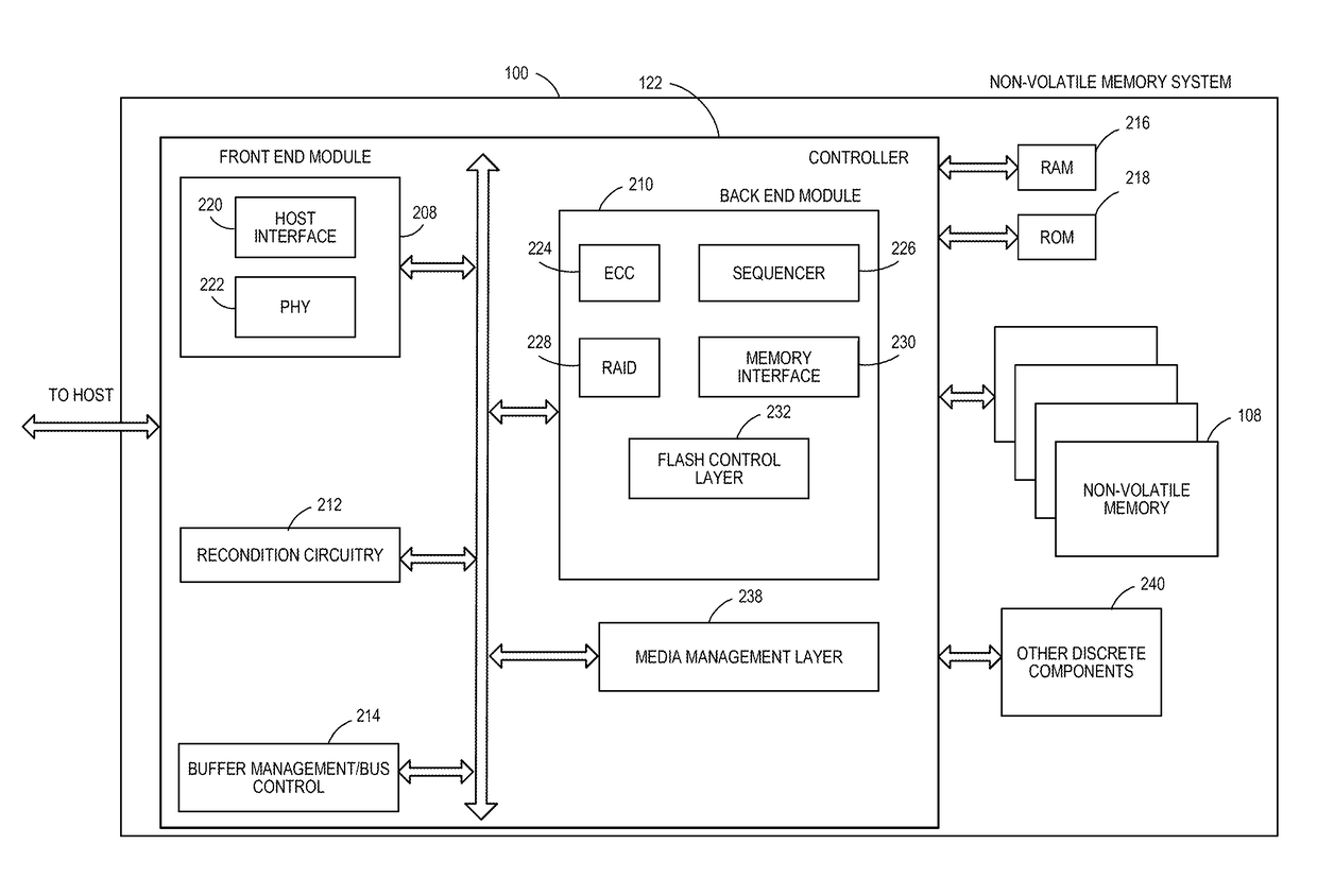
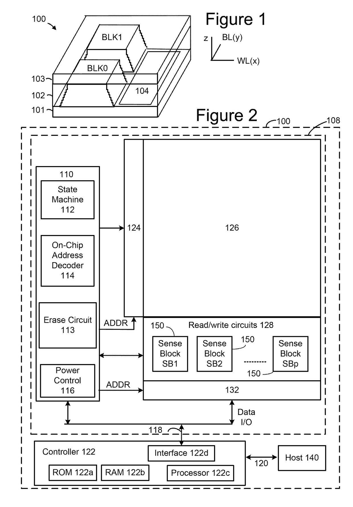
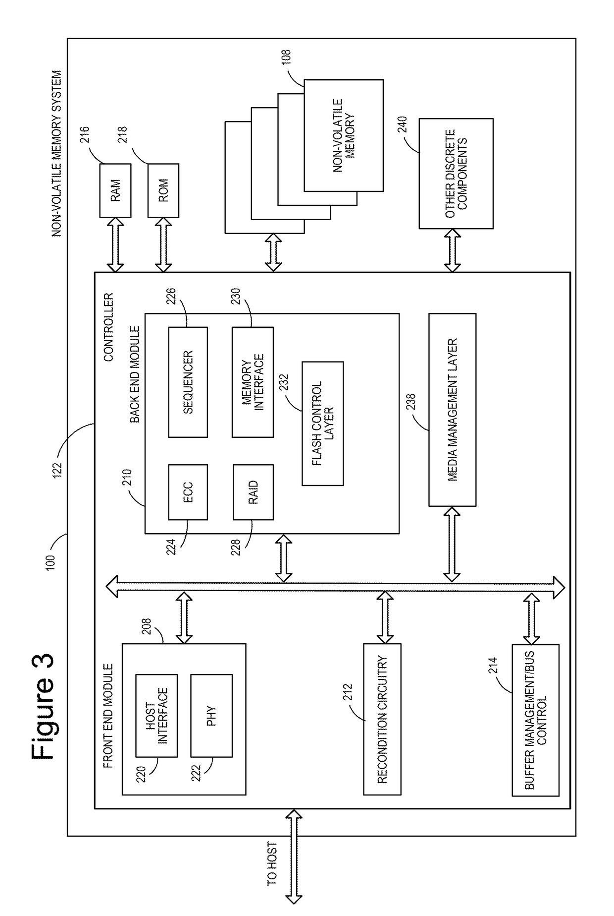
[0032]The disclosed technology is directed to improved erase operations in non-volatile memory. A group of non-volatile memory cells such as a block is erased and subjected to erase verification. When the block is successfully verified as erased, an erase depth check is performed for a subset of memory cells of the block. If the subset of memory cells fails the erase depth check, the block or a portion of the block can be subjected to further erasing. In this manner, an additional operation to determine an erase level of a subset of memory cells is provided to detect the occurrence of shallow erased memory cells at the end of the erase process. If a shallow erase condition is detected for the subset of memory cells, the block or a portion of the block undergoes additional erasing to reduce the shallow erase condition. By detecting and eliminating shallow erased memory cells, errors when sensing data that is subsequently programmed to the non-volatile memory can be reduced.

[0033]Bloc...


PUM


Abstract

An erase operation includes one or more erase depth checks to detect the occurrence of shallow erased memory cells at the end of an erase process. Memory cells are subjected to erase and erase verification until erase verification success is achieved. At the end of successful erase verification, a subset of memory cells is read to detect an erase depth or level of the memory cells. If the erase depth check indicates that the subset memory cells are in a shallow erased condition, additional erasing and verification is performed.

Description

BACKGROUND OF THE INVENTION[0001]Semiconductor memory devices have become more popular for use in various electronic devices. For example, non-volatile semiconductor memory is used in cellular telephones, digital cameras, personal digital assistants, mobile computing devices, non-mobile computing devices and other devices. Flash memory is among the most popular non-volatile semiconductor memories.[0002]Some non-volatile memory devices are used to store two ranges of charges and, therefore, the memory cells can be programmed / erased between two data states: an erased state and a programmed state (corresponding to data “1” and data “0”). Such a device is referred to as a binary device or a single-level cell (SLC) and the data is binary data.[0003]A multi-state flash memory cell (storing multi-state data) is implemented by identifying multiple, distinct allowed threshold voltage ranges (ie data states). Each distinct threshold voltage range corresponds to a predetermined value for the s...

Claims


Application Information

Patent Timeline
IPC IPC(8): G11C16/34G11C16/10G11C16/28G11C16/04G11C16/16
CPCG11C16/3431G11C16/3495G11C16/16G11C16/28G11C16/0483G11C16/10G11C16/3418G11C16/344G11C16/3445G11C16/3459
Inventor RAY, BISWAJITDUNGA, MOHANCHEN, CHANGYUAN
Owner SANDISK TECH LLC
Why Eureka
Try Eureka