
Wafer processing method

Active Publication Date: 2018-05-03
DISCO CORP
View PDF8 Cites 3 Cited by
  • Summary
  • Abstract
  • Description
  • Claims
  • Application Information

AI Technical Summary

Benefits of technology

The present invention provides a method for efficiently processing wafers to create individual device chips without compromising device quality. This method involves stacking multiple layers on the front side of the wafer, including a functional layer with multiple devices separated by crossing division lines. This approach eliminates the need for multiple laser processed grooves on the front side of the wafer, which improves productivity. The back side of each device chip can also be held under suction and easily picked up from the adhesive tape. The front side of each chip can then be bonded to a wiring board, further improving productivity.

Problems solved by technology

As a result, there is a problem that the productivity may be reduced.
Furthermore, the following problems have been found in performing the method described in Japanese Patent Laid-open No. 2005-064231.
(1) When the removal of the functional layer from each division line is insufficient in performing laser grooving such that the laser beam is applied to the front side of the wafer to remove the functional layer from each division line, the cutting blade may be deviated or tilted or uneven wearing of the cutting blade may occur in dicing the wafer after laser grooving.
(2) When the laser beam is applied to the front side of the wafer to form the laser processed grooves in laser grooving, debris may scatter and stick to the front side of the wafer, causing a degradation in device quality.
Accordingly, a protective film must be formed on the front side of the wafer, causing a reduction in productivity.

Method used


Image

  • Wafer processing method
  • Wafer processing method
  • Wafer processing method

Examples


Embodiment Construction

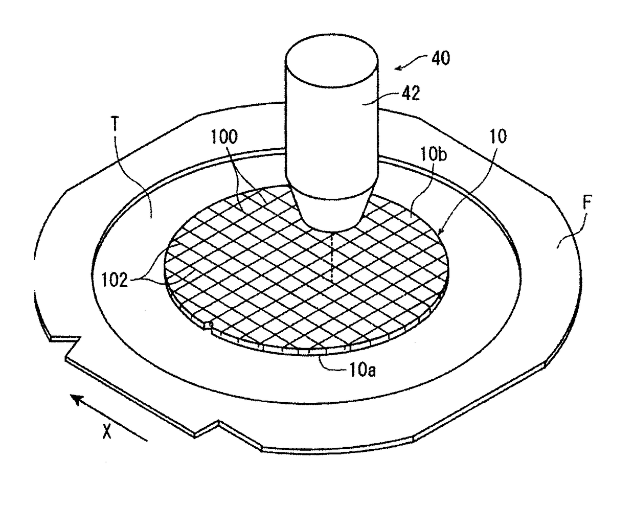
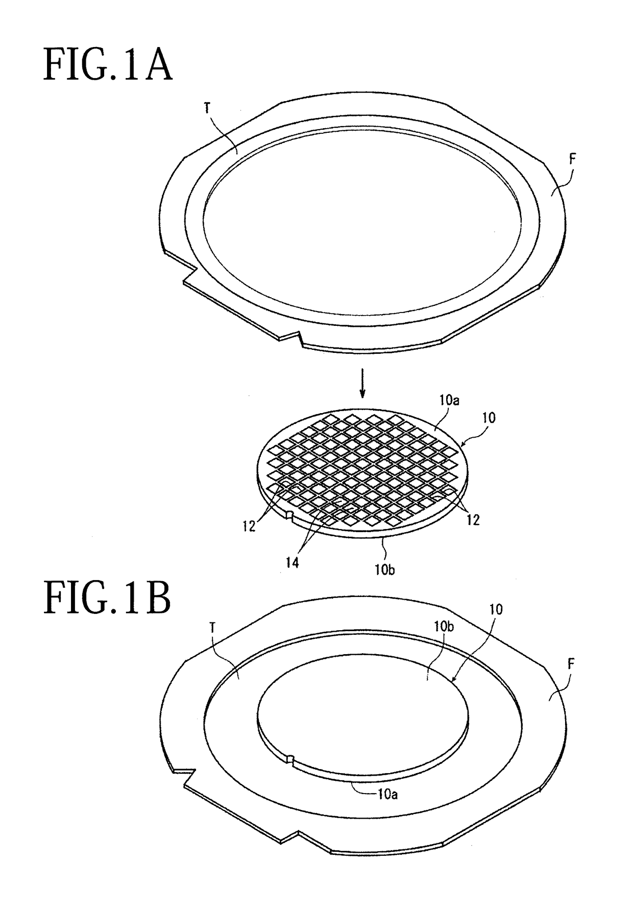
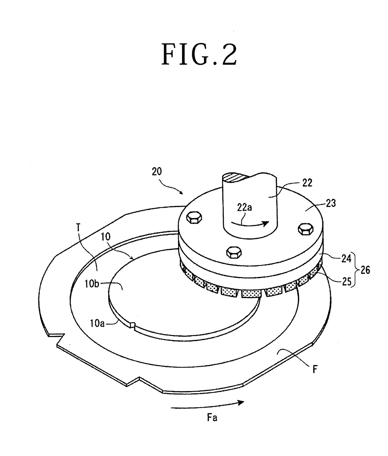
[0026]A preferred embodiment of the wafer processing method according to the present invention will now be described in detail with reference to the attached drawings. FIGS. 1A and 1B illustrate a wafer supporting step of supporting a wafer 10 through an adhesive tape T to an annular frame F. More specifically, as illustrated in FIG. 1A, the wafer 10 has a front side 10a and a back side 10b. The adhesive tape T is attached to the front side 10a of the wafer 10. A peripheral portion of the adhesive tape T is previously attached to an annular frame F having an inside opening for receiving the wafer 10. That is, the inside opening of the annular frame F is closed by a central portion of the adhesive tape T, and this central portion of the adhesive tape T is attached to the front side 10a of the wafer 10. Thus, the wafer 10 is supported through the adhesive tape T to the annular frame F. After supporting the wafer 10 through the adhesive tape T to the annular frame F, the back side 10b ...


PUM


Abstract

A wafer processing method divides a wafer into individual device chips along division lines. The method includes attaching an adhesive tape to the front side of the wafer and attaching a peripheral portion of the adhesive tape to an annular frame having an inside opening for receiving the wafer, thereby supporting the wafer through the adhesive tape to the annular frame; grinding the back side of the wafer to reduce the thickness of the wafer; cutting the back side of the wafer along each division line by using a cutting blade to form a cut groove having a depth not reaching the front side of the wafer; and applying a laser beam to the bottom of the cut groove from the back side of the wafer along each division line to divide the wafer to obtain the individual device chips.

Description

BACKGROUND OF THE INVENTIONField of the Invention[0001]The present invention relates to a wafer processing method for dividing a wafer into a plurality of individual device chips along a plurality of division lines, the division lines being formed on the front side of the wafer to thereby define a plurality of separate regions where a plurality of devices are individually formed.Description of the Related Art[0002]A plurality of devices such as integrated circuits (ICs), large-scale integration (LSI) circuits are formed on the front side of a wafer so as to be separated by a plurality of crossing division lines. The wafer thus having the devices on the front side is divided into individual device chips along the division lines by using a dicing apparatus having a cutting blade. These device chips are used in various electrical equipment such as mobile phones and personal computers.[0003]In recent years, increasing the processing speed of each device has been desired and it is known ...

Claims


Application Information

Patent Timeline
IPC IPC(8): H01L21/78H01L21/268H01L21/683
CPCH01L21/78H01L21/2686H01L21/6836H01L2221/68327B23K26/402B24B19/22B24B41/06B28D5/0058B28D5/0082B28D5/022H01L21/02016H01L21/02013H01L21/76B23K26/38H01L21/67132H01L21/67712H01L21/67721
Inventor YAMASHITA, YOHEIOBATA, TSUBASAOGAWA, YUKI
Owner DISCO CORP
Learn More