Semiconductor device and manufacturing method thereof

a technology of semiconductors and semiconductors, applied in the direction of semiconductor devices, basic electric elements, electrical equipment, etc., can solve problems such as structural distortion, such as bending of stacked structures, and achieve the effect of reducing manufacturing costs and improving manufacturing efficiency

Active Publication Date: 2018-05-10
SK HYNIX INC
View PDF3 Cites 38 Cited by
  • Summary
  • Abstract
  • Description
  • Claims
  • Application Information

AI Technical Summary

Problems solved by technology

However, structural distortion, such as bending of the stacked structure, may occur during the manufacturing processes of the three-dimensional semiconductor device.

Method used


Image

  • Semiconductor device and manufacturing method thereof
  • Semiconductor device and manufacturing method thereof
  • Semiconductor device and manufacturing method thereof

Examples


Embodiment Construction

[0027]Hereinafter, various exemplary embodiments of the present invention will be described in detail with reference to the accompanying drawings. Various modifications and changes may be applied to the illustrated exemplary embodiments. In addition, other embodiments including changes, equivalents, or alternatives thereof may be envisaged by those skilled in the art to which the present invention pertains after reading the present disclosure without departing from the spirit and technical scope of the present invention.

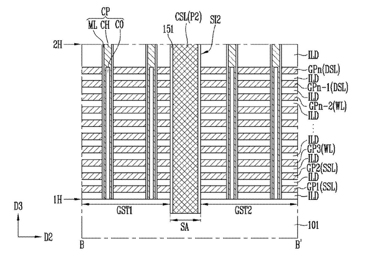
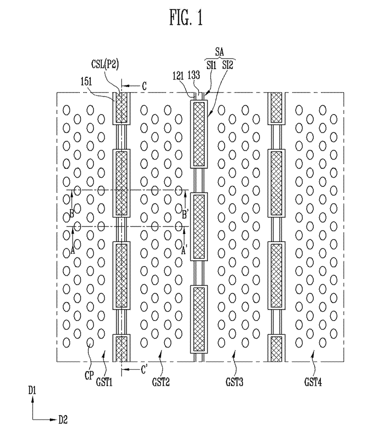
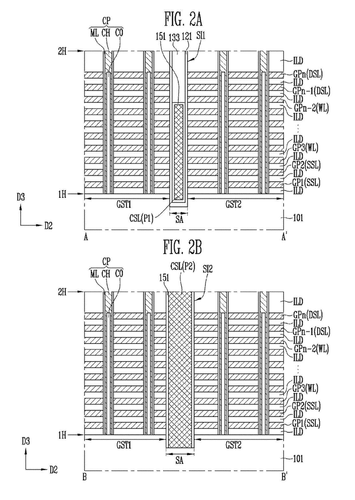
[0028]Various embodiments of the present invention are directed to an improved three-dimensional semiconductor memory device having an enhanced structural stability and a manufacturing method thereof.

[0029]It will be understood that, although the terms “first”, “second”, “third”, and so on may be used herein to describe various elements, these elements are not limited by these terms. These terms are used to distinguish one element from another element. Thus, a first ...


PUM


Abstract

A semiconductor device includes gate stacked structures surrounding channel layers, a common source line filling a separation area between the gate stacked structures adjacent to each other and having an upper surface including first concave portions, and a support insulating layer filling the first concave portions and having sidewalls facing portions of the channel layers.

Description

CROSS-REFERENCE TO RELATED APPLICATION[0001]The present application claims priority under 35 U.S.C. § 119(a) to Korean patent application number 10-2016-0148176, filed on Nov. 8, 2016, the entire disclosure of which is incorporated herein by reference in its entirety.BACKGROUNDField of Invention[0002]Various embodiments of the invention relate generally to a semiconductor device and a manufacturing method thereof, and more particularly, to a semiconductor device including a stacked structure and a method of manufacturing the same.Description of Related Art[0003]A semiconductor device may include memory cells storing data. The memory cells of the semiconductor device may be arranged in three dimensions to obtain a higher degree of integration. A three-dimensional semiconductor device including the three-dimensionally arranged memory cells may include a stacked structure surrounding a channel layer. The stacked structure may include interlayer insulating layers and conductive patterns...

Claims


Application Information

Patent Timeline
Patent Type & Authority Applications(United States)
IPC IPC(8): H01L27/11568H01L27/11582H01L27/11565
CPCH01L27/11568H01L27/11565H01L27/11582H10B41/20H10B41/27H10B43/20H10B43/27H10B43/35H10B43/10H10B41/50H10B43/50H10B43/30
Inventor LEE, KI HONG
Owner SK HYNIX INC
Why Eureka
Try Eureka