Ceramic electronic device

a technology of electronic devices and ceramics, applied in the direction of fixed capacitor details, stacked capacitors, fixed capacitors, etc., to achieve the effect of preventing acoustic noise, enhancing the reduction effect of stress, and preventing an acoustic nois

Active Publication Date: 2018-07-26
TDK CORPARATION
View PDF6 Cites 7 Cited by
  • Summary
  • Abstract
  • Description
  • Claims
  • Application Information

AI Technical Summary

Benefits of technology

[0037]The first through hole and the second through hole have any opening width in the width direction, but when the second through hole has a larger opening width, the metal terminal portion can effectively enhance a reduction effect on stress and a prevention effect on acoustic noise. When the first through hole has an opening width that is narrower than an opening width of the second through hole, a connection strength between the chip components and the electrode face portion using the connection member or so can be prevented from being excessively high, and such a ceramic electronic device can prevent an acoustic noise.

Problems solved by technology

However, a conventional metal terminal with a link portion between a mount portion and a connection portion (electrode face portion) has a problem that a ceramic electronic device has a mount area (a projected area in the Z-axis direction) that is larger to some degree than a projected area of a chip component.

Method used


Image

  • Ceramic electronic device
  • Ceramic electronic device
  • Ceramic electronic device

Examples


first embodiment

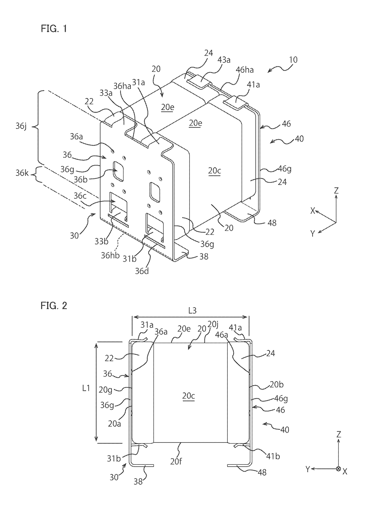
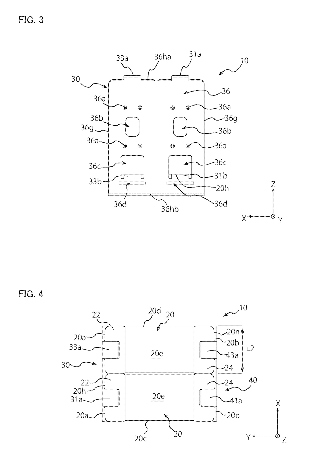
[0054]FIG. 1 is a schematic perspective view showing a ceramic capacitor 10 according to First Embodiment of the present invention. The ceramic capacitor 10 has chip capacitors 20 as chip components and a pair of metal terminal portions 30 and 40. The ceramic capacitor 10 according to First Embodiment has the two chip capacitors 20, but the ceramic capacitor 10 has any plural chip capacitors 20.

[0055]Incidentally, each embodiment is described with a ceramic capacitor where the chip capacitors 20 are equipped with the metal terminal portions 30 and 40, but the ceramic electronic device of the present invention is not limited to the ceramic capacitor, and may be a chip component other than capacitors equipped with the metal terminal portions 30 and 40. In the description of each embodiment, as shown in FIG. 1 to FIG. 11, the X-axis direction is a direction where first side surfaces 20c and second side surfaces 20d of the chip capacitors 20 are connected (a parallel direction to chip s...

second embodiment

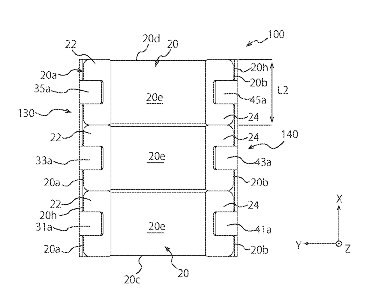
[0107]FIG. 7 is a schematic perspective view of a ceramic capacitor 100 according to Second Embodiment of the present invention. FIG. 8 to FIG. 11 are respectively a front view, a left side view, a top view, and a bottom view of the ceramic capacitor 100. As shown in FIG. 7, the ceramic capacitor 100 is similar to the ceramic capacitor 10 according to First Embodiment except that the ceramic capacitor 100 has three chip capacitors 20 and a different number of first through holes 36b or so contained in a first metal terminal portion 130 and a second metal terminal portion 140. In the description of the ceramic capacitor 100, similar parts to the ceramic capacitor 10 are provided with similar references to the ceramic capacitor 10 and are not described.

[0108]As shown in FIG. 7, the chip capacitors 20 contained in the ceramic capacitor 100 are similar to the chip capacitors 20 contained in the ceramic capacitor 10 shown in FIG. 1. The three chip capacitors 20 contained in the ceramic c...

example

[0121]

[0122]5.0×6.0×6.4 mm

[0123]

[0124]Size: (L3×L1×L2) 5.7×5.0×2.5 mm

[0125]Capacitance: 15 μF

[0126]

[0127]Material: three-layer clad material Cu—NiFe—Cu

[0128]Size of electrode face portion 36: (Z-axis direction (terminal first side 36g)×X-axis direction (terminal second side 36ha)×plate thickness) 6.3×5.0×0.1 mm

[0129]Size of arm 33a: (X direction×Y direction) 0.9×0.9 mm

[0130]Size of mount portion: (Y direction) 1.2 mm

[0131]

[0132]Frequency: 100 Hz to 10 MHz

[0133]Temperature: 25° C.


PUM

PropertyMeasurementUnit
thicknessaaaaaaaaaa
thicknessaaaaaaaaaa
thicknessaaaaaaaaaa

Abstract

A ceramic electronic device includes multiple chip components and a pair of metal terminal portions. The chip components consist of a pair of chip end surfaces and four chip side surfaces. Terminal electrodes are formed on the pair of chip end surfaces. The pair of metal terminal portions is arranged correspondingly with the pair of chip end surfaces. Each of the pair of metal terminal portions includes an electrode face portion, multiple pairs of engagement arm portions, and a mount portion. The electrode face portion faces the chip end surface. The multiple pairs of engagement arm portions extend from the electrode face portion toward the chip side surface and sandwich and hold the chip components. The mount portion extends from one of terminal second sides toward the chip components and is partially substantially vertical to the electrode face portion.

Description

BACKGROUND OF THE INVENTION1. Field of the Invention[0001]The present invention relates to a ceramic electronic device having a chip component and a metal terminal attached thereto.2. Description of the Related Art[0002]In addition to a normal chip component that is solely directly mounted on a board or so, a chip component attached with a metal terminal is proposed as a ceramic electronic device, such as a ceramic capacitor. It is reported that the ceramic electronic device attached with a metal terminal after being mounted has a reduction effect on a deformation stress that travels from a board to a chip component and a protection effect on a chip component from impacts or so. Thus, the ceramic electronic device attached with a metal terminal is used in a field where durability, reliability, and the like are required.[0003]It is also reported that a metal terminal has a prevention effect on a vibration generated in the chip component from traveling to a mount board. To enhance suc...

Claims


Application Information

Patent Timeline
Patent Type & Authority Applications(United States)
IPC IPC(8): H01G4/248H01G4/38H01G4/30H01G4/232
CPCH01G4/248H01G4/38H01G4/30H01G4/232H01G4/008H01G2/065H01G4/1227H01G2/06H01G4/12H01G4/228
Inventor ANDO, NORIHISAKOBAYASHI, KATSUMIMASUDA, SUNAOMORI, MASAHIROMATSUNAGA, KAYOUYAZAWA, KOSUKE
Owner TDK CORPARATION
Why Eureka
Try Eureka