Antenna device and electronic apparatus

an antenna device and electronic equipment technology, applied in the structure of radiating elements, near-field systems using receivers, transmission, etc., can solve the problems of reducing the proportion of magnetic flux contributing to weakening the magnetic coupling between the feed coil and the coil antenna of the communication partner, etc., to achieve the effect of increasing the coupling coefficient and reducing the size and thickness

Active Publication Date: 2018-07-26
MURATA MFG CO LTD
View PDF1 Cites 66 Cited by
  • Summary
  • Abstract
  • Description
  • Claims
  • Application Information

AI Technical Summary

Benefits of technology

[0013]An electronic apparatus according to a preferred embodiment of the present invention includes an antenna device and a casing. The antenna device includes a circuit substrate, a feed circuit, a coil antenna, a wiring pattern, a planar first conductive pattern, a planar second conductive pattern, and a connection conductor. The coil antenna is mounted on the circuit substrate. The wiring pattern is disposed on the circuit substrate and connects the coil antenna and the feed circuit. The first conductive pattern is disposed on the circuit substrate and located outside a loop current path defined by the coil antenna, the feed circuit, and the wiring pattern when the circuit substrate is seen in plan view. The second conductive pattern is disposed on the circuit substrate and located inside the loop current path when the circuit substrate is seen in plan view. The connection conductor or the wiring pattern connects the first conductive pattern and the second conductive pattern in at least two locations and is disposed on the circuit substrate. At least one location of the connection conductor includes an interlayer connection conductor. With this configuration, the electronic apparatus achieving the above-described advantageous effects is obtained.
[0014]According to preferred embodiments of the present invention, antenna devices and electronic apparatuses including the same are able to achieve reductions in size and thickness and have an increased coefficient of coupling between the coil antennas thereof and a coil antenna of a communication partner.

Problems solved by technology

Unfortunately, however, some magnetic flux expands in unnecessary directions through the gap, and the proportion of magnetic flux contributing to the magnetic coupling between the feed coil and the coil antenna of the communication partner decreases.
This leads to weakening of the magnetic coupling between the feed coil and the coil antenna of the communication partner.

Method used


Image

  • Antenna device and electronic apparatus
  • Antenna device and electronic apparatus
  • Antenna device and electronic apparatus

Examples


first preferred embodiment

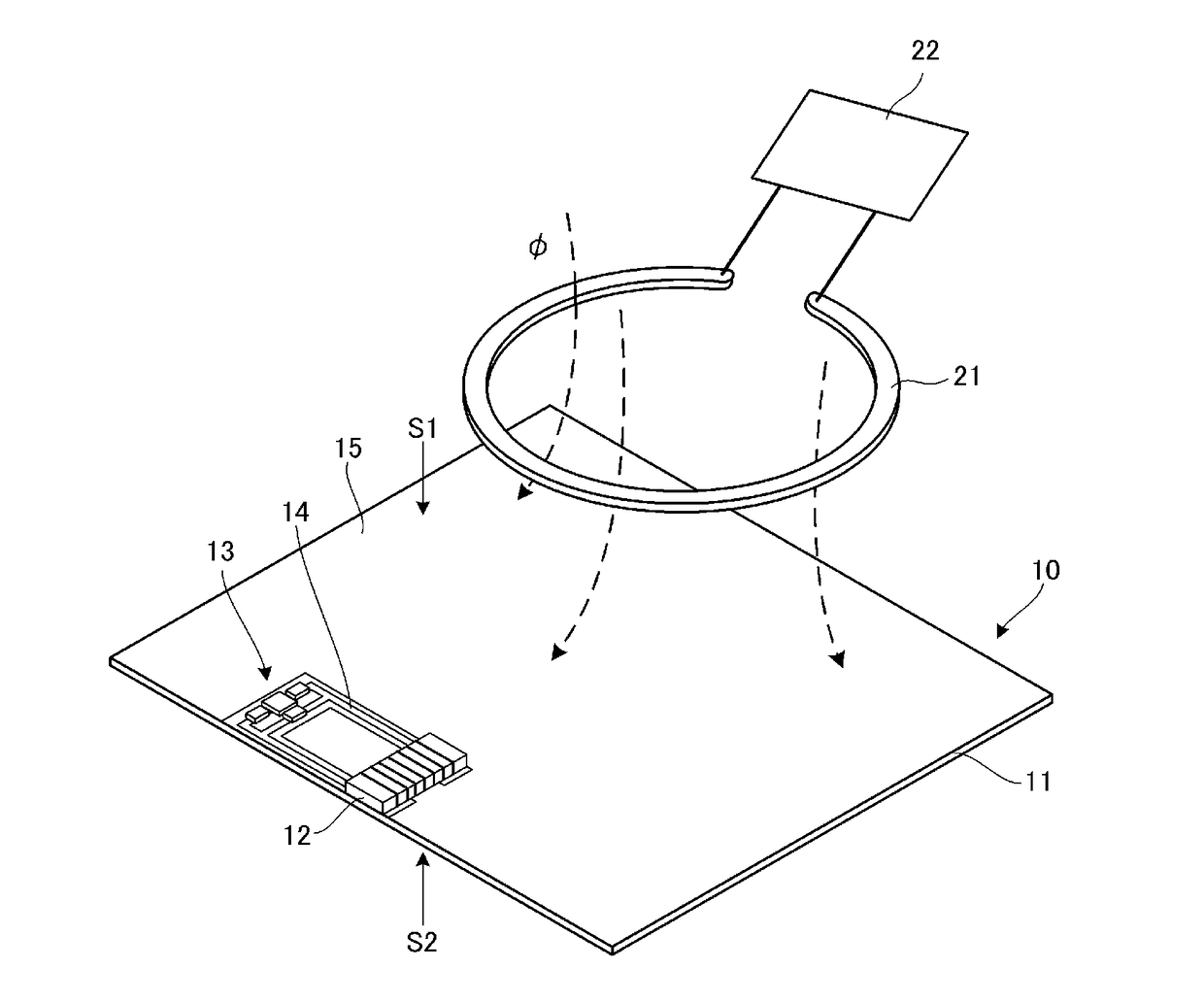
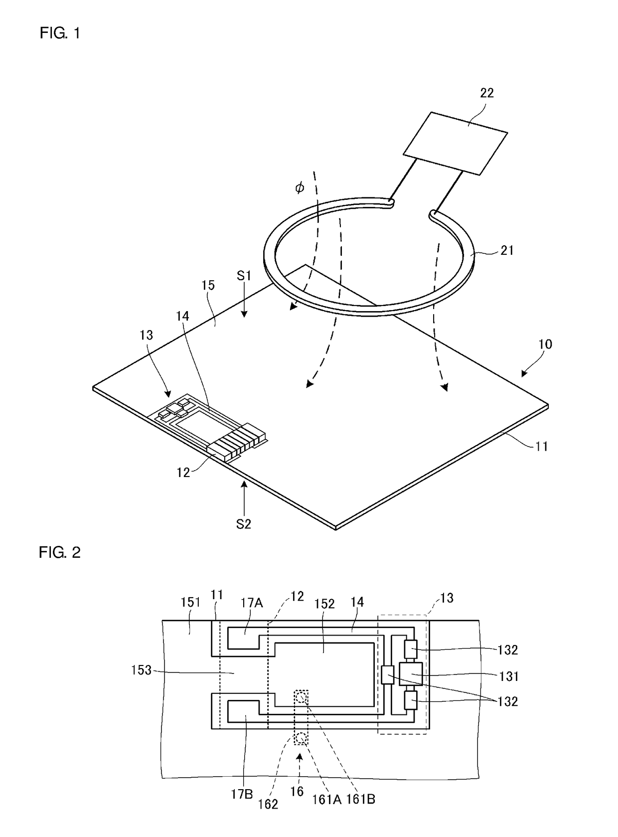
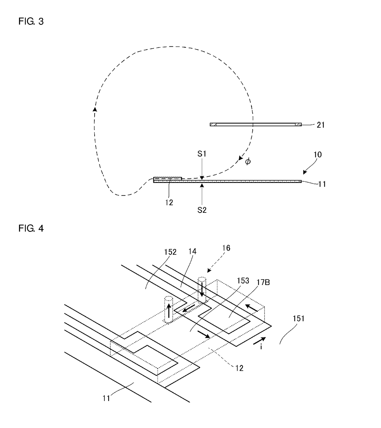
[0026]FIG. 1 is a perspective view of an antenna device and a coil antenna of a communication partner according to a first preferred embodiment. FIG. 2 is a plan view of a main portion of the antenna device according to the first preferred embodiment. FIG. 3 is a cross-sectional view that illustrates a portion of magnetic flux produced by the coil antenna of the communication partner. FIG. 4 is a perspective view that illustrates an eddy current generated by magnetic flux expanding through a gap between a wiring pattern 14 and conductive patterns 151 and 152. The directions of magnetic flux illustrated in FIGS. 1 and 3 indicate the ones when a current flows in a predetermined direction in the coil antenna of the communication partner.

[0027]An antenna device 10 includes a circuit substrate 11, a coil antenna 12, a feed circuit 13, the wiring pattern 14, a conductive pattern 15, and a connection conductor 16. The coil antenna 12 is mounted on a first principal surface S1 of the circui...

second preferred embodiment

[0038]An electronic apparatus according to a second preferred embodiment of the present invention includes a casing and an antenna device arranged inside the casing. FIG. 5 is a plan view that illustrates a structure inside the casing of the electronic apparatus including the antenna device according to the second preferred embodiment. The electronic apparatus is preferably a communication terminal apparatus, such as a smartphone, for example. A casing 41 houses circuit substrates 31A and 31B, a battery pack 42, and other elements. The coil antenna 12 and feed circuit 13 are provided on the circuit substrate 31A. That is, the wiring pattern 14, the conductive pattern 15, and the connection conductor 16 are provided on the circuit substrate 31A. The antenna device having the same or substantially the same configuration as in the first preferred embodiment is arranged inside the casing 41. The circuit substrate 31A is provided with an ultrahigh frequency (UHF) antenna 43, a camera mod...

third preferred embodiment

[0040]In a first example of a third preferred embodiment of the present invention, the first conductive pattern and second conductive pattern are connected to each other only by connection conductors including interlayer connection conductors. FIG. 6A is a plan view of a main portion of an antenna device according to the first example of the third preferred embodiment. The first conductive pattern 151 and second conductive pattern 152 are connected to each other in two locations by the connection conductor 16 and a connection conductor 58. The connection conductor 58 is disposed on the circuit substrate 11 so as to overlap the coil antenna 12 when seen in plan view.

[0041]The connection conductor 58 includes interlayer connection conductors 581A and 581B and a linear conductive pattern 582. The conductive pattern 582 is disposed on the second principal surface of the circuit substrate 11. The interlayer connection conductor 581A overlaps the conductive patterns 151 and 582 when seen ...


PUM


Abstract

A coil antenna is mounted on a circuit substrate. A wiring pattern is disposed on the circuit substrate and connects the coil antenna and a feed circuit. A conductive pattern is disposed on the circuit substrate and located outside a region surrounded by the coil antenna, feed circuit, and wiring pattern. A conductive pattern is disposed on the circuit substrate and located inside the region surrounded by the coil antenna, feed circuit, and wiring pattern. Connection conductors connect the conductive pattern and conductive pattern and are disposed on the circuit substrate. The connection conductor includes interlayer connection conductors.

Description

CROSS REFERENCE TO RELATED APPLICATIONS[0001]This application claims the benefit of priority to Japanese Patent Application No. 2015-210798 filed on Oct. 27, 2015 and is a Continuation Application of PCT Application No. PCT / JP2016 / 081665 filed on Oct. 26, 2016. The entire contents of each application are hereby incorporated herein by reference.BACKGROUND OF THE INVENTION1. Field of the Invention[0002]The present invention relates to an antenna device in a near field communication (NFC) system or other systems and an electronic apparatus including the same.2. Description of the Related Art[0003]An example of a known antenna device used in the NFC system is described in Japanese Unexamined Patent Application Publication No. 2014-75775. This antenna device includes a feed coil and a planar conductor. The feed coil is connected to a radio frequency integrated circuit (RFIC). The planar conductor has a slit extending from a portion of its outer edge toward its inner area. The feed coil i...

Claims


Application Information

Patent Timeline
Patent Type & Authority Applications(United States)
IPC IPC(8): H04B5/00H01Q7/00H01Q1/38
CPCH04B5/0081H01Q7/00H01Q1/38H01Q1/06H01Q1/243H04B5/02
Inventor TENNO, NOBUYUKI
Owner MURATA MFG CO LTD
Why Eureka
Try Eureka