Light source device

a technology of light source and semiconductor, applied in the direction of semiconductor lasers, lighting and heating apparatus, instruments, etc., can solve the problem of inability to suppress the temperature increase of semiconductor laser elements b>1011/b>, and achieve the effect of adequately achieving thermal dissipation performance, efficiently dissipating heat generated, and preventing the performance of nitride semiconductor laser elements from decreasing

Active Publication Date: 2018-08-16
PANASONIC SEMICON SOLUTIONS CO LTD
View PDF0 Cites 2 Cited by
  • Summary
  • Abstract
  • Description
  • Claims
  • Application Information

AI Technical Summary

Benefits of technology

[0039]With this configuration, even when a nitride semiconductor laser element that is relatively high in operating voltage is used, thermal dissipation performance can be adequately achieved. Thus, performance of the nitride semiconductor laser element can be prevented from decreasing.
[0040]The present disclosure can provide a light source device that can efficiently dissipate heat generated by a semiconductor light-emitting device.

Problems solved by technology

In this case, due to a lack of the thermal dissipation performance of semiconductor laser device 1010, temperature increase of semiconductor laser element 1011 cannot be suppressed.

Method used


Image

  • Light source device
  • Light source device
  • Light source device

Examples


embodiment 1

Variation 4 of Embodiment 1

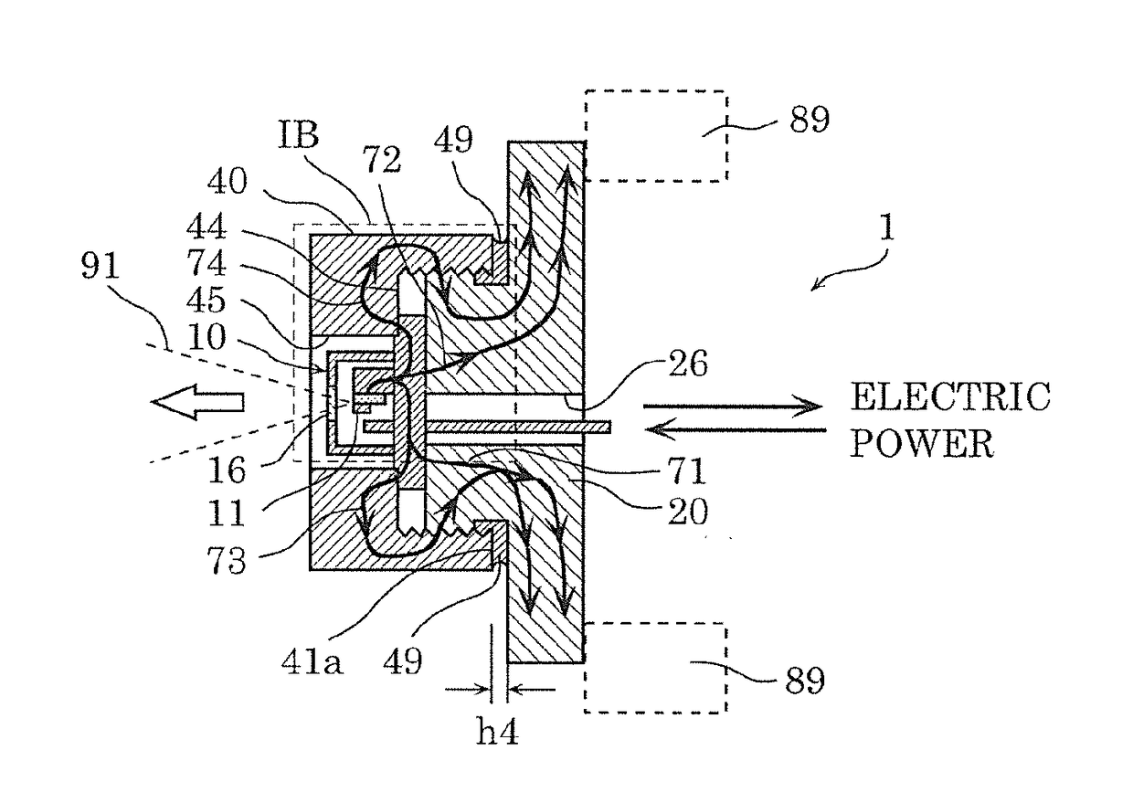
[0134]Hereinafter, a light source device according to Variation 4 of Embodiment 1 is described. The light source device according to the present variation is different from light source device 1 according to Embodiment 1 in configuration of a base, a first pressing surface, and a second pressing surface. The following mainly describes differences between the light source device according to the present variation and light source device 1 according to Embodiment 1, with reference to the drawing.

[0135]FIG. 10 is a schematic cross-sectional view showing a configuration of main components of light source device 1d according to the present variation.

[0136]As shown in FIG. 10, light source device 1d according to the present variation is different from light source device 1 according to Embodiment 1 in that first projection 44d and second projection 24d are formed, respectively, in first pressing surface 44 of first fixing component 40d and second pressing surfac...

embodiment 2

[0138]Hereinafter, a light source device according to Embodiment 2 is described. Light source device 101 according to the present embodiment is different from light source device 1a according to Variation 1 of Embodiment 1 in that a filler is used and that a lens module for collecting emission light is provided. The following mainly describes differences between light source device 101 according to the present embodiment and light source device 1a according to Variation 1 of Embodiment 1, with reference to the drawings.

[0139]FIG. 11 is an exploded schematic cross-sectional view showing a configuration of light source device 101 according to the present embodiment.

[0140]FIG. 12 is a schematic cross-sectional view showing a configuration of light source device 101 according to the present embodiment.

[0141]As shown in FIG. 11, before semiconductor light-emitting device 10 is attached to second fixing component 20a, filler 148 is applied to a bottom surface of base recess 23 formed in s...

embodiment 3

[0147]Hereinafter, a light source device according to Embodiment 3 is described. The light source device according to the present embodiment has a configuration in which a wavelength conversion member including a phosphor or the like is added to light source device 101 according to Embodiment 2. The following describes a configuration and an operation of the light source device according to the present embodiment.

[Configuration]

[0148]Firstly, a configuration of the light source device according to the present embodiment is described, with reference to the drawings.

[0149]FIG. 13 is a schematic cross-sectional view showing a configuration of light source device 201 according to the present embodiment.

[0150]FIG. 14 is an exploded schematic cross-sectional view showing a configuration of light source device 201 according to the present embodiment.

[0151]FIG. 15 is a schematic exploded perspective view showing a configuration of light source device 201 according to the present embodiment....


PUM


Abstract

A light source device includes: a semiconductor light-emitting device including a flat-shaped base having a first main surface on a first side and a second main surface and a semiconductor light-emitting element disposed on the first side; a first fixing component having a first through-hole and a first pressing surface that presses the first main surface; and a second fixing component having a second through-hole and a second pressing surface that presses the second main surface. The base is fixed between the first and second pressing surfaces by an engagement between a first inner surface surrounding the first through-hole of the first fixing component and a second outer surface of the second fixing component. A distance between the first and second pressing surfaces is smaller than or equal to a thickness of the base, and a void is formed lateral to the base between the first and second pressing surfaces.

Description

CROSS REFERENCE TO RELATED APPLICATIONS[0001]This application is a U.S. continuation application of PCT International Patent Application Number PCT / JP2016 / 004587 filed on Oct. 14, 2016, claiming the benefit of priority of Japanese Patent Application Number 2015-206677 filed on Oct. 20, 2015, the entire contents of which are hereby incorporated by reference.BACKGROUND1. Technical Field[0002]The present disclosure relates to light source devices, and particularly to a light source device which includes a semiconductor light-emitting device and is used for, for example, a projection display device, vehicle lighting, and facility lighting.2. Description of the Related Art[0003]A light source device which includes a semiconductor light-emitting device packaged with a semiconductor light-emitting element, such as a semiconductor laser, is known as an example of a conventional light source device (see Japanese Unexamined Patent Application Publication No. 2001-358398, for example). Such a ...

Claims


Application Information

Patent Timeline
Patent Type & Authority Applications(United States)
IPC IPC(8): H05B33/08G03B21/20G02B27/09F21V17/04F21V19/00H05B44/00H01S5/02315H01S5/0233
CPCH05B33/0803G03B21/2033G02B27/0955F21V17/04F21V19/003F21V19/0015G02B27/0977H01S5/02H01S5/02212H01S5/02469G02B19/0052G02B19/0028G02B19/0014G03B21/16H01S5/02257H01S5/0087H01S5/02438H01S5/02315H01S5/0233H01S5/02208H01S5/02476H01S5/024H01S5/0235
Inventor YAMANAKA, KAZUHIKOMORIMOTO, KIYOSHIKASUGAI, HIDEKIMATSUMURA, KAZUYUKIYAMAGUCHI, HIDEOSUZUKI, NOBUYASU
Owner PANASONIC SEMICON SOLUTIONS CO LTD
Why Eureka
Try Eureka