Liquid crystal display panel and liquid crystal display apparatus having the same

a liquid crystal display and applied in the field of liquid crystal display technology, can solve problems such as poor display effect, and achieve the effect of high contras

Inactive Publication Date: 2018-08-30
SHENZHEN CHINA STAR OPTOELECTRONICS SEMICON DISPLAY TECH CO LTD
View PDF10 Cites 1 Cited by
  • Summary
  • Abstract
  • Description
  • Claims
  • Application Information

AI Technical Summary

Benefits of technology

[0047]The beneficial effect of the present invention is: compared with the conventional liquid crystal display panel, the polar angles of liquid crystal molecules in two adjacent rows of pixels in the liquid crystal display panel of the present invention are different, which further forms an image of pixels with alternately-arranged bright rows and dark rows. Thus, the adjacent rows of pixels have higher contrast when watching at a large viewing angle, thereby solving the technical problem of color-shift at larger viewing angle.

Problems solved by technology

The present invention provides a liquid crystal display panel, wherein the polar angles of liquid crystal molecules in two adjacent rows of pixels in a multi-domain vertical alignment type liquid crystal display panel are different, which solves a technical problem that the display image of a conventional multi-domain vertical alignment type panel has a decreased contrast and a color-shift problem when watching at a large viewing angle, thereby leading to a poor display effect.

Method used


Image

  • Liquid crystal display panel and liquid crystal display apparatus having the same
  • Liquid crystal display panel and liquid crystal display apparatus having the same
  • Liquid crystal display panel and liquid crystal display apparatus having the same

Examples


first embodiment

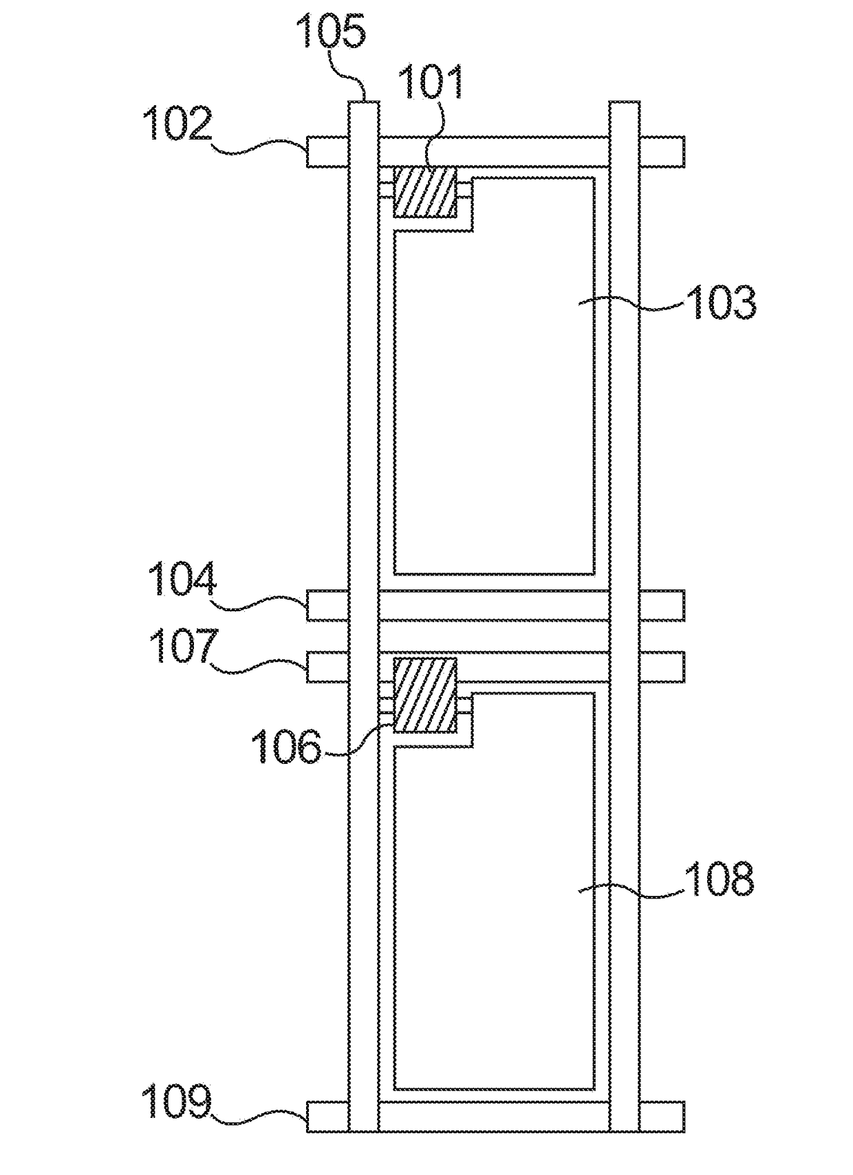
[0055]FIG. 1 is a schematic diagram of a pixel structure according to a first embodiment of the present invention.

[0056]As shown in FIG. 1, the embodiment of the present invention uses an odd-numbered row pixel and an even-numbered row pixel which are adjacent in a pixel unit as an example for description.

[0057]A sub-pixel of the odd-numbered row pixel includes a first thin-film transistor 101, a first scanning line 102, a first pixel electrode 103 and a first common line 104. The first common line 104 is substantially parallel with the first scanning line 102. The first pixel electrode 103 is disposed between the first scanning line 102 and the first common line 104. A data line 105 is perpendicularly crossed with the first scanning line 102 and the first common line 104. A gate of the first thin-film transistor 101 is connected to the first scanning line 102. A source of the first thin-film transistor 101 is connected to the data line 105. A drain of the first thin-film transistor...

second embodiment

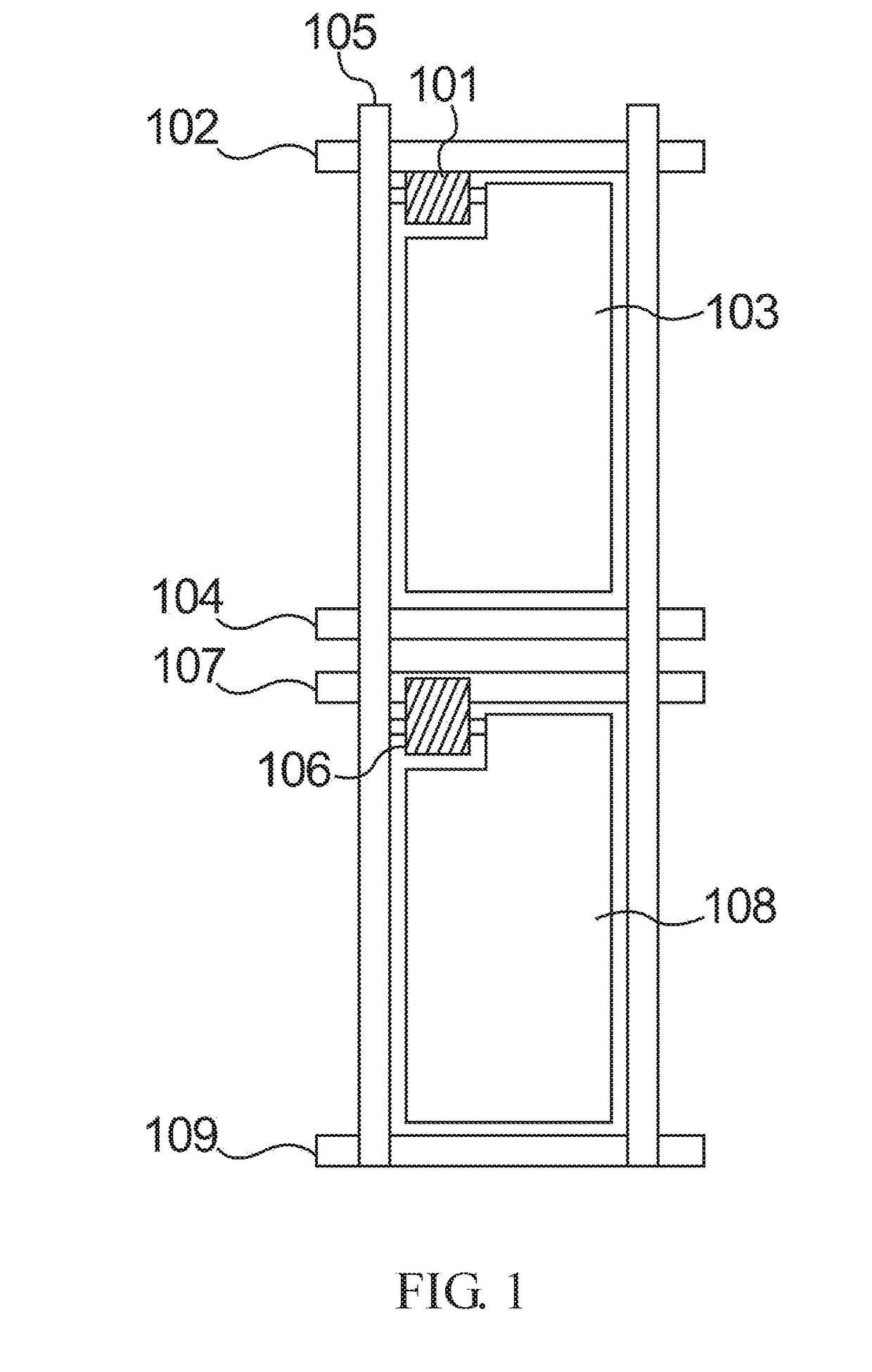
[0062]FIG. 2 is a schematic diagram of a pixel structure according to a second embodiment of the present invention.

[0063]As shown in FIG. 2, the embodiment of the present invention uses an odd-numbered row pixel and an even-numbered row pixel which are adjacent in a pixel unit as an example for description.

[0064]A sub-pixel of the odd-numbered row pixel includes a first thin-film transistor 201, a first scanning line 202, a first pixel electrode 203, and a first common line 204. The first common line 204 is substantially parallel with the first scanning line 202. The first pixel electrode 203 is disposed between the first scanning line 202 and the first common line 204. A data line 205 is perpendicularly crossed with the first scanning line 202 and the first common line 204. A gate of the first thin-film transistor 201 is connected to the first scanning line 202. A source of the first thin-film transistor 201 is connected to the data line 205. A drain of the first thin-film transist...

third embodiment

[0071]FIG. 3 is a schematic diagram of a pixel structure according to a second embodiment of the present invention.

[0072]As shown in FIG. 3, the embodiment of the present invention uses an odd-numbered row pixel and an even-numbered row pixel which are adjacent in a pixel unit as an example for description.

[0073]A sub-pixel of the even-numbered row pixel includes a second thin-film transistor 306, a second scanning line 307, a second pixel electrode 308, and a second common line 309. The second common line 309 is substantially parallel with the second scanning line 307. The second pixel electrode 308 is disposed between the second scanning line 307 and the second common line 309. A data line 305 is perpendicularly crossed with the second scanning line 307 and the second common line 309. A gate the second thin-film transistor 306 is connected to the second scanning line 307. A source of the second thin-film transistor 306 is connected to the data line 305. A drain of the second thin-...


PUM

PropertyMeasurementUnit
viewing-angleaaaaaaaaaa
voltageaaaaaaaaaa
polar anglesaaaaaaaaaa

Abstract

The present invention provides a liquid crystal display panel having: a plurality of odd-numbered row pixels and a plurality of even-numbered row pixels that are alternately arranged. A voltage value of a pixel electrode to which the odd-numbered row pixels or the even-numbered row pixels correspond is adjusted so as to form different polar angles of liquid crystal molecules at the odd-numbered row pixels and the even-numbered row pixels. The beneficial effect of the is that, in the liquid crystal display panel, the polar angles of liquid crystal molecules in the adjacent row pixels are different to solve the technical problem of color-shift at large viewing angles.

Description

BACKGROUND OF THE INVENTIONField of the Invention[0001]The present invention relates to the technical field of liquid crystal display technology, and more particularly to a liquid crystal display panel and a liquid crystal display apparatus having the same.Description of the Related Art[0002]A liquid crystal display (LCD) with advantages such as lightweight and thin-structure has gradually become one of the fastest developing flat-panel display devices. However, compared with a cathode ray tube display, the viewing angle of a thin-film transistor LCD is relatively narrow, which greatly limits the possible applications in the technical field of high-end display with strict requirements of viewing angle, such as aerospace technology or medical technology. With the fast development of wide-viewing angle technology in the technical field of LCD, currently there are many products with a viewing-angle characteristic that is able to reach 85 degrees or even larger for both the horizontal v...

Claims


Application Information

Patent Timeline
Patent Type & Authority Applications(United States)
IPC IPC(8): G02F1/1362G02F1/1335G02F1/1368G02F1/1337G02F1/137
CPCG02F1/136286G02F1/133514G02F1/1368G02F1/136213G02F1/133707G02F1/137G02F2201/123G02F1/133753G02F1/13624G09G3/3637G09G2300/0439G09G2300/0447G09G3/3614G09G3/3648H01L29/78696
Inventor HAO, SIKUN
Owner SHENZHEN CHINA STAR OPTOELECTRONICS SEMICON DISPLAY TECH CO LTD
Why Eureka
Try Eureka