
Display device and method for manufacturing display device

Active Publication Date: 2018-10-11
JAPAN DISPLAY INC
View PDF2 Cites 4 Cited by
  • Summary
  • Abstract
  • Description
  • Claims
  • Application Information

AI Technical Summary

Benefits of technology

The goal of this patent is to prevent distortion in the display quality caused by electrical charges leaking into nearby pixels.

Problems solved by technology

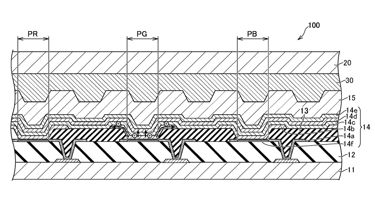
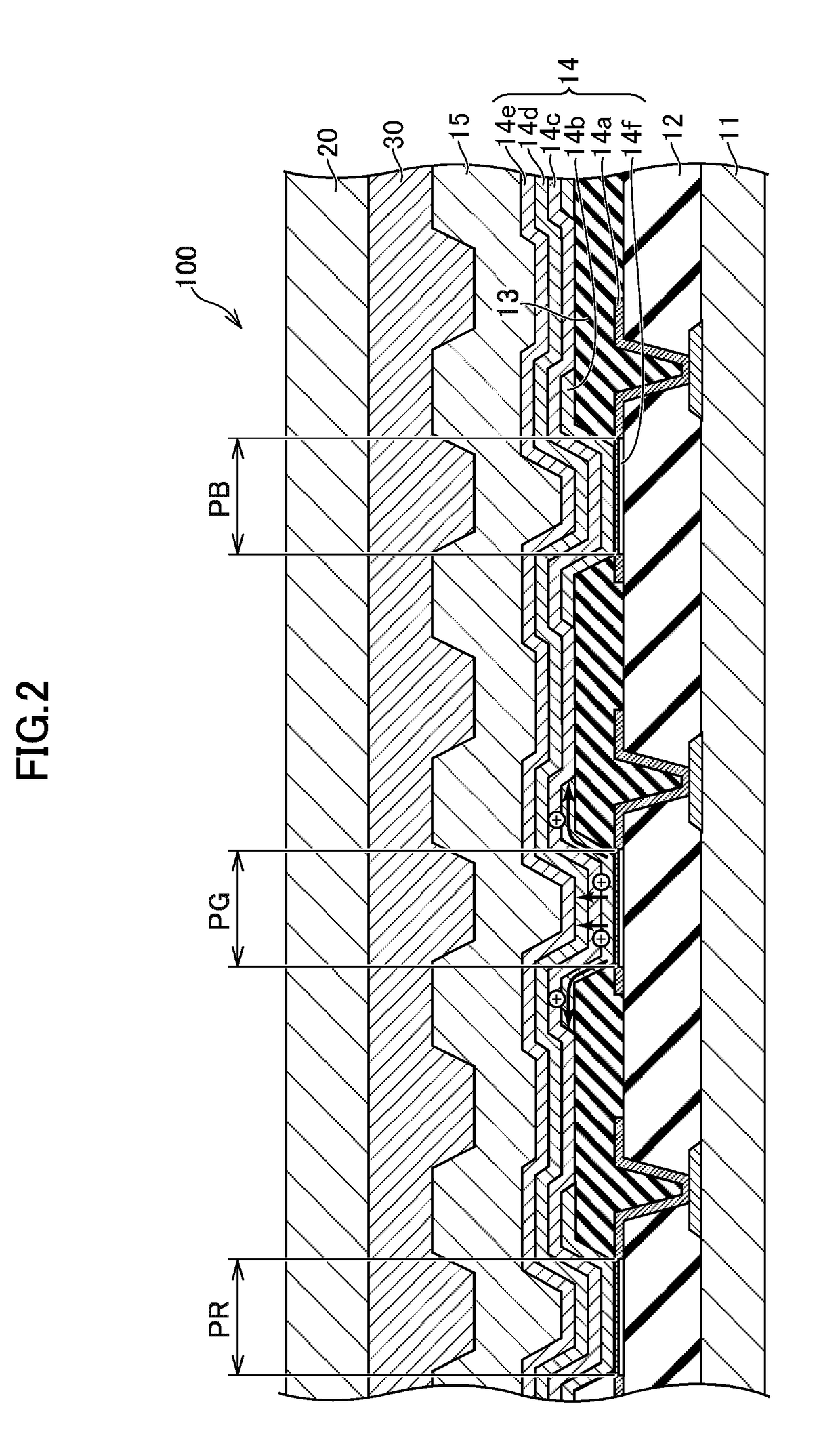
When such a hole transport layer containing p-dopant is formed across pixels, charge may leak into an adjacent pixel, which possibly causes unintended light emission from the adjacent pixel.
Resultantly, color mixture (electric color mixture) may result, and display quality may be possibly deteriorated.

Method used


Image

  • Display device and method for manufacturing display device
  • Display device and method for manufacturing display device
  • Display device and method for manufacturing display device

Examples


Embodiment Construction

[0015]The following describes an embodiment of the present invention (hereinafter referred to as this embodiment) while referring to the drawings. The present invention can be rendered into practice in various aspects without departing from the gist of the present invention. The present invention should not be interpreted as being limited to the description of the embodiment below.

[0016]The respective widths, thicknesses, shapes, and so forth may be illustrated more schematically in the drawings, compared with actual widths, thicknesses, shapes, and so forth in order to make clearer the description of the present invention. These, however, are mere examples, and should not limit interpretation of the present invention in any way. In the specification and drawings, any elements having the same functions as those having been described earlier with respect to a drawing referred to earlier are given the same reference numerals, and may not be described in detail again.

[0017]In the detai...


PUM


Abstract

To provide a display device including a plurality of pixels; a light emitting element layer formed across the plurality of pixels; and a bank formed so as to separately define adjacent pixels among the plurality of pixels, wherein the light emitting element layer includes a p-doped hole transport layer containing p-dopant, and the p-doped hole transport layer is formed on each of the pixels such that the p-doped hole transport layers on the respective adjacent pixels are separated from each other on the bank.

Description

CROSS-REFERENCE TO RELATED APPLICATION[0001]The present application claims priority from Japanese application JP2017-078020 filed on Apr. 11, 2017, the content of which is hereby incorporated by reference into this application.BACKGROUND OF THE INVENTION1. Field of the Invention[0002]The present invention relates to display devices, and a method for manufacturing the display devices.2. Description of the Related Art[0003]Some display devices include a light emitting element layer including a lower electrode (an anode electrode), a light emissive layer formed on the lower electrode, and an upper electrode (a cathode electrode) formed on the light emissive layer. A light emitting element layer formed across a plurality of pixels is known. A light emitting element layer including a hole transport layer for transporting holes from a lower electrode to a light emissive layer is known. A hole transport layer containing p-dopant including organic material is known (for example, JP2004-5371...

Claims


Application Information

Patent Timeline
IPC IPC(8): H01L51/50H01L27/32H01L51/00H01L51/56
CPCH01L51/506H01L27/3246H01L51/5064H01L51/002H01L51/56H01L2227/323H10K59/35H10K59/122H10K50/156H10K50/155H10K71/00H10K71/30H10K59/1201
Inventor TOYODA, HIRONORI
Owner JAPAN DISPLAY INC
Learn More