
Bulk acoustic wave resonator and method of manufacturing the same

a technology of acoustic waves and resonators, which is applied in the direction of impedence networks, electrical devices, etc., can solve the problems of increasing the size of an overall filter device, increasing the size of a respective resonator, and increasing the constraints of structure and process design

Active Publication Date: 2018-10-25
SAMSUNG ELECTRO MECHANICS CO LTD
View PDF0 Cites 15 Cited by
  • Summary
  • Abstract
  • Description
  • Claims
  • Application Information

AI Technical Summary

Benefits of technology

The patent describes a way to make a bulk acoustic wave resonator that stops the membrane layer from sticking to the substrate. This patent also explains how to make the resonator using a specific method.

Problems solved by technology

Also, as sacrificial layer thicknesses are further reduced, there is a high possibility that resonant portions and substrates may be stuck during manufacturing processes, increasing constraints on structures and process designs.
However, increasing the thickness of a sacrificial layer unconditionally may not be feasible in terms of a manufacturing process.
However, as the thickness of a sacrificial layer increases, the length of an inclined surface of the sacrificial layer also increases, which leads to an increase in the size of an overall filter device, as well as, a respective resonator.
In addition, as the thickness of the sacrificial layer increases, characteristic deterioration may be easily caused due to an increase in a length of a connection portion between resonators.
Furthermore, because increasing the thickness of a sacrificial layer causes an increase in a size of a step to correspond to the increased thickness in a subsequent process, a problem of negative properties in terms of process accuracy may occur.

Method used


Image

  • Bulk acoustic wave resonator and method of manufacturing the same
  • Bulk acoustic wave resonator and method of manufacturing the same
  • Bulk acoustic wave resonator and method of manufacturing the same

Examples


Embodiment Construction

[0036]The following detailed description is provided to assist the reader in gaining a comprehensive understanding of the methods, apparatuses, and / or systems described herein. However, various changes, modifications, and equivalents of the methods, apparatuses, and / or systems described herein will be apparent after an understanding of the disclosure of this application. For example, the sequences of operations described herein are merely examples, and are not limited to those set forth herein, but may be changed as will be apparent after an understanding of the disclosure of this application, with the exception of operations necessarily occurring in a certain order. Also, descriptions of features that are known in the art may be omitted for increased clarity and conciseness.

[0037]The features described herein may be embodied in different forms, and are not to be construed as being limited to the examples described herein. Rather, the examples described herein have been provided mer...


PUM


Abstract

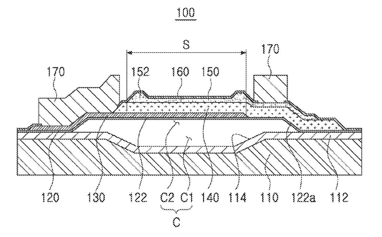
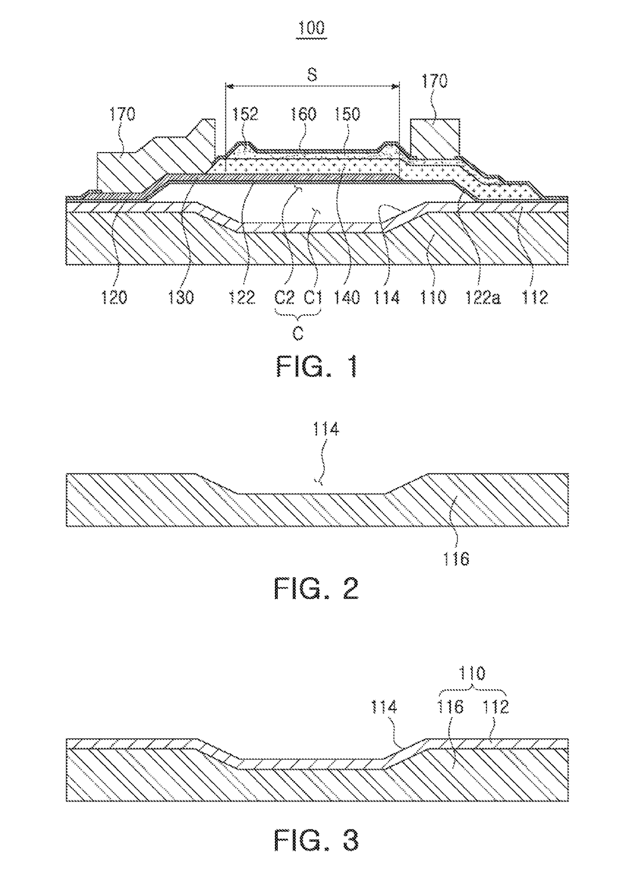
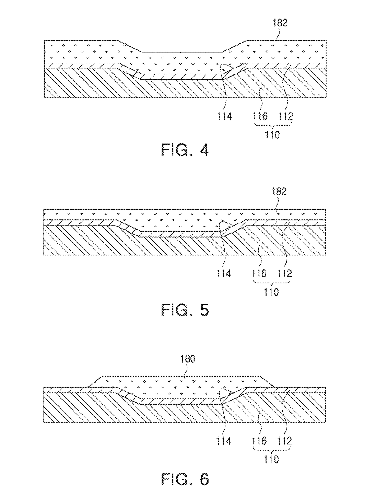
A bulk acoustic wave resonator includes a substrate including a cavity groove, a membrane layer disposed above the substrate and including a convex portion. And a lower electrode including a portion thereof disposed on the convex portion. The bulk acoustic wave resonator also includes a piezoelectric layer configured so that a portion of the piezoelectric layer is disposed above the convex portion, and an upper electrode disposed on the piezoelectric layer. A first space formed by the cavity groove and a second space formed by the convex portion form a cavity, the cavity groove is disposed below an active region, and the convex portion comprises an inclined surface disposed outside of the cavity groove.

Description

CROSS-REFERENCE TO RELATED APPLICATION(S)[0001]This application claims benefit under 35 USC 119(a) of priority to Korean Patent Application No. 10-2017-0050608 filed on Apr. 19, 2017 in the Korean Intellectual Property Office, the disclosure of which is incorporated herein by reference in its entirety.BACKGROUND1. Field[0002]The following description relates to a bulk acoustic wave resonator and a method of manufacturing the same.2. Description of Related Art[0003]In general, a space, which may be secured for resonance in bulk acoustic resonators, is determined by thicknesses of sacrificial layers.[0004]Also, as sacrificial layer thicknesses are further reduced, there is a high possibility that resonant portions and substrates may be stuck during manufacturing processes, increasing constraints on structures and process designs.[0005]On the other hand, as the thicknesses of sacrificial layers increase, the possibility of occurrence of stiction between resonant portions and substrates...

Claims


Application Information

Patent Timeline
Patent Type & Authority Applications(United States)
IPC IPC(8): H03H9/17H03H9/02H03H9/05
CPCH03H9/173H03H9/02015H03H9/0514H03H3/02H03H9/02007H03H9/17H03H9/02118H03H2003/021H03H9/25H03H9/02614H03H9/564H03H9/172H03H9/174H03H9/02094
Inventor LIM, CHANG HYUNPARK, YOON SOKKIM, JONG WOONKIM, TAE YOONLEE, MOON CHUL
Owner SAMSUNG ELECTRO MECHANICS CO LTD
Learn More