

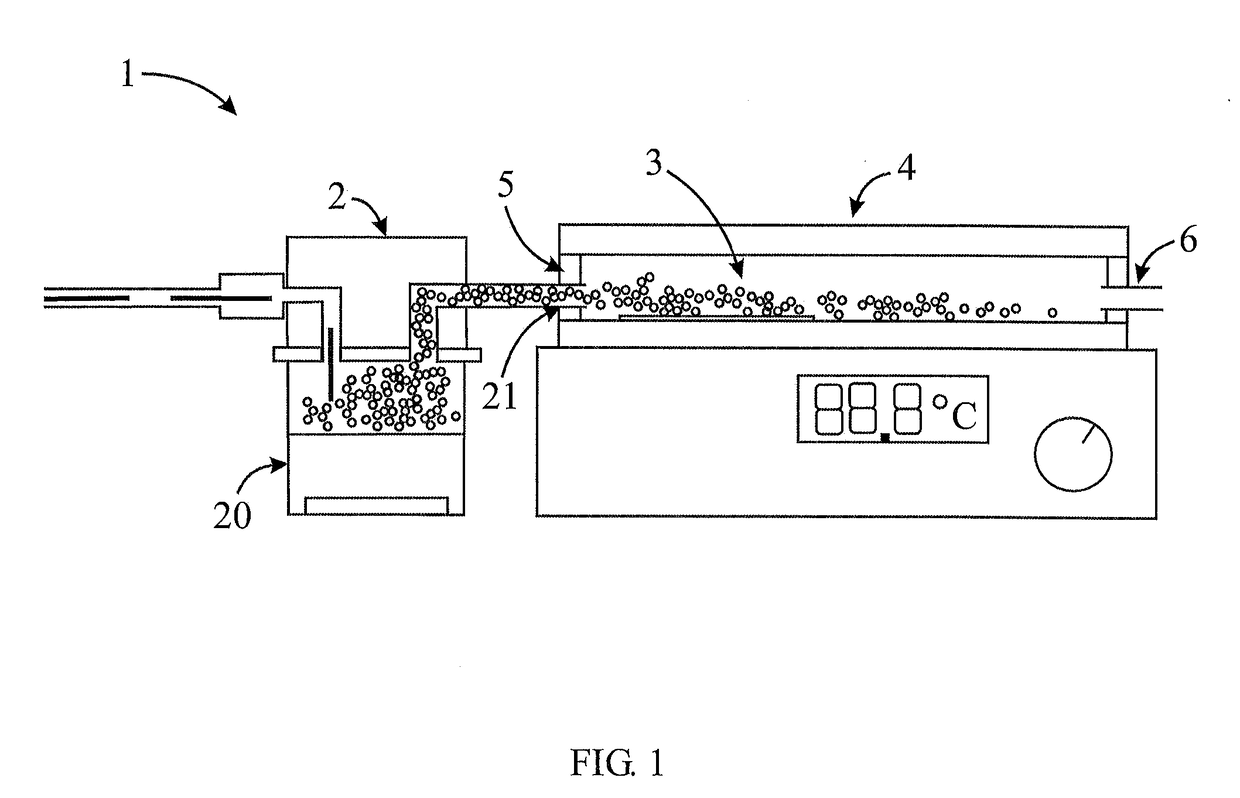
Apparatus and method for aerosol deposition of nanoparticles on a substrate
a technology of nanoparticles and aerosols, applied in the field of printing electronics, can solve the problems of severely degrading the electrical performance of transistor devices, majority of these systems are not adapted to ultrathin films, etc., and achieve the effect of minimizing the impact of relative humidity changes and minimizing hysteresis
- Summary
- Abstract
- Description
- Claims
- Application Information
AI Technical Summary
Benefits of technology
Problems solved by technology
Method used
Image

Examples
examples
[0073]The effect of modifying the intensity of the electric field in the deposition chamber on the deposition of carbon nanotubes on the substrate was examined. As shown in FIG. 5, seven injector nozzles were used to deposit single-walled carbon nanotubes on a silicon substrate. The seven injector nozzles gave rise to the seven horizontal deposition patterns shown in the top section of FIG. 5a. From right to left, the applied voltage varied from +2400 V to −2400 V in steps of 200 V, which corresponds to 25 different conditions. Between each voltage, the sample was translated 600 μm in the horizontal direction. At the highest fields, isolated dark stripes were clearly visible, with lateral dimensions below 100×600 μm2. As the field weakens, the deposition pattern spreads until the laminar flow from neighboring nozzles prevents further spreading. This is clearer in FIG. 5b which was taken under different illumination conditions. It should be noted that when the field is absent (vertic...
PUM
| Property | Measurement | Unit |
|---|---|---|
| Water contact angle | aaaaa | aaaaa |
| Water contact angle | aaaaa | aaaaa |
| Water contact angle | aaaaa | aaaaa |
Abstract
Description
Claims
Application Information