Light emitting diode (LED) test apparatus and method of manufacture

a technology of light emitting diodes and test apparatus, applied in the field of mass-production scale manufacturing, can solve the problems of low yield and reliability of led devices, test reliability, and test reliability of probe pin cards having hundreds or even thousands of probe pins, and achieve the effect of reducing cost and reducing yield

Active Publication Date: 2019-01-03
APPLE INC
View PDF0 Cites 21 Cited by
  • Summary
  • Abstract
  • Description
  • Claims
  • Application Information

AI Technical Summary

Benefits of technology

[0005]During the LED manufacturing process, LED structures are formed on a substrate using mass-production processes like those utilized by the semiconductor industry. Process steps such as cleaning, deposition, lithography, etching and metallization are used to form the basic LED structure. To achieve mass-production scale manufacturing and lower cost, numerous devices are simultaneously formed on a substrate using these processes. Different substrates and materials are used depending on the type of LED desired. For example, UV-emitting LEDs are typically made from Gallium Nitride

Problems solved by technology

The device size and sheer volume of individual LED devices on a substrate makes this a challenging task.
This process almost always produces contact pad scratches that can lower LED device yield and reliability.
Test reliability, fabrication and maintenance costs of using probe pin cards having hundreds o

Method used


Image

  • Light emitting diode (LED) test apparatus and method of manufacture
  • Light emitting diode (LED) test apparatus and method of manufacture
  • Light emitting diode (LED) test apparatus and method of manufacture

Examples


embodiment 1500

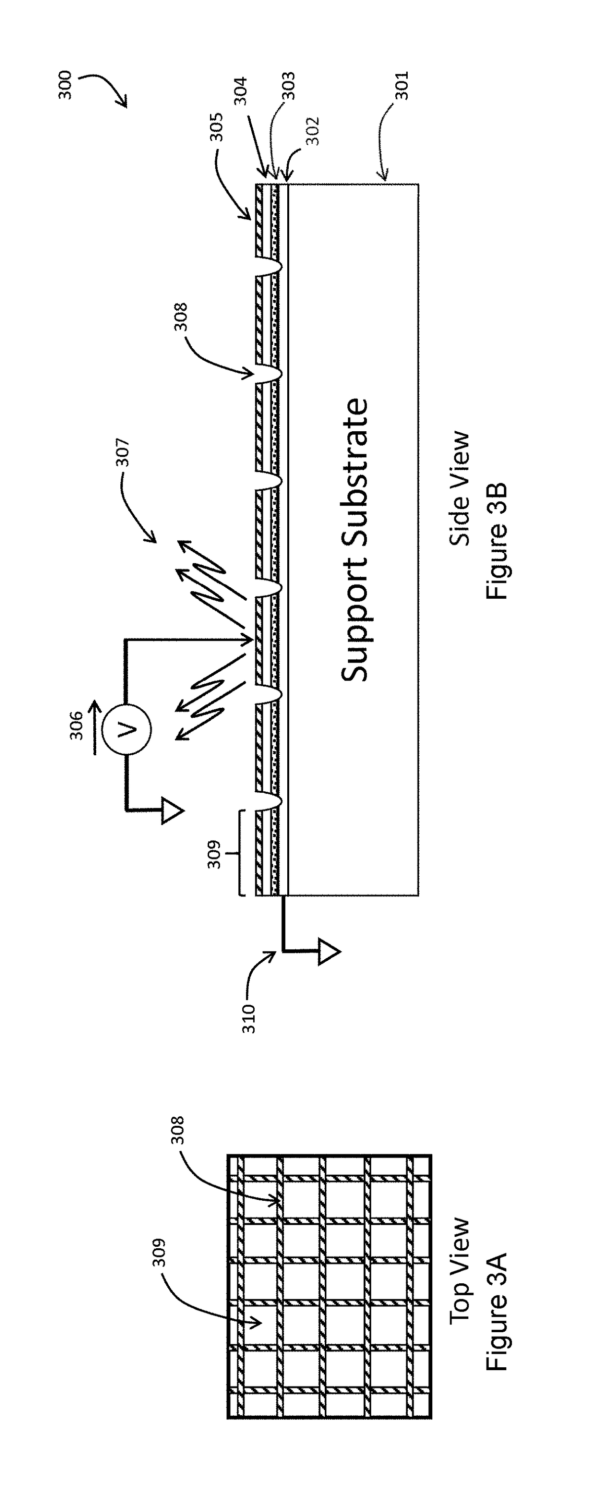
[0132]Although this invention has been described with a common contact existing under the LED devices, other current injection configurations are possible. FIG. 15A shows another embodiment 1500 where an analogue to the field plate 1501 is present within support substrate 1502 below the plurality of LED device structures such as LED device 1503. Under the lowest LED device structure layer (the n-layer in examples described in this invention), a dielectric layer 1504 and electrode 1505 completes the support substrate capacitive coupling device. Electrode 1505 is connected to a voltage source 1506. The field plate is connected to a separate voltage source 1507 and field plate electrode 1508. In this example, a camera 1509 is placed above the field plate to capture the light emission response of the plurality of LED devices under test. In this example, the isolation between devices is shown to be complete, however this method would still function with or without full isolation of the n...

embodiment 1600

[0133]In yet another embodiment, C2I functional testing could also be applied to a modification of the test configuration of FIG. 15A that eliminates the need for a buried electrode within the support substrate. In this embodiment, the dielectric property of the support substrate itself is used to inject current through the LED devices. For example, a quartz, sapphire, glass or plastic support substrate could serve as dielectric 1504 in FIG. 15A. FIG. 16 shows a specific embodiment 1600 of this configuration. A support substrate 1601 having adequate dielectric properties and thickness containing a plurality of LED devices on its surface such as LED device 1602 is placed on top of an electrode 1603 connected to a voltage source 1606. Although not shown specifically, a gap can exist between electrode 1603 and support substrate 1601, allowing non-contact operation of the back side of the support substrate if desired. Although not shown specifically, an additional dielectric can also be...


PUM


Abstract

Embodiments relate to functional test methods useful for fabricating products containing Light Emitting Diode (LED) structures. In particular, LED arrays are functionally tested by injecting current via a displacement current coupling device using a field plate comprising of an electrode and insulator placed in close proximity to the LED array. A controlled voltage waveform is then applied to the field plate electrode to excite the LED devices in parallel for high-throughput. A camera records the individual light emission resulting from the electrical excitation to yield a function test of a plurality of LED devices. Changing the voltage conditions can excite the LEDs at differing current density levels to functionally measure external quantum efficiency and other important device functional parameters. Spectral filtering is used to improve measurement contrast and LED defect detection. External light irradiation is used to excite the LED array and improve onset of charge injection light emission and throughput.

Description

[0001]This application is a nonprovisional of U.S. Patent Application No. 62 / 522,576 filed Jun. 20, 2017, the contents of which are incorporated by reference herein.FIELD OF INVENTION[0002]The present invention relates to light emitting diode (LED) devices. More particularly, embodiments of the invention relate to techniques, including methods and apparatus to functionally test a Light Emitting Diode (LED) array structure during the manufacturing process. In an example, the method is useful in general LED device functional testing and is particularly useful for functionally testing micro-LED (uLED) devices that can be as small as a few microns on a side. Micro-LEDs are grown on a support substrate utilizing techniques such as Metallo-Organic Chemical Vapor Deposition (MOCVD) among others. Before the individual devices are used in their final lighting or display application, it is desirable to test the LED devices to achieve one or more of the following: yield evaluation, binning, de...

Claims


Application Information

Patent Timeline
IPC IPC(8): G01R31/26H01L33/62G01R29/08G01R31/00H05B44/00
CPCG01R31/2635H01L33/62G01R29/0821G01R31/002G01R31/312G01R31/3025H01L33/0095H01L27/156H10N35/101
Inventor HENLEY, FRANCOIS J.
Owner APPLE INC
Why Eureka
Try Eureka