Thermoelectric conversion element, method for manufacturing thermoelectric conversion element, thermoelectric conversion module, and method for manufacturing thermoelectric conversion module

a technology of thermoelectric conversion element and thermoelectric conversion module, which is applied in the direction of thermoelectric device details, thermoelectric device manufacture/treatment, solid-state device, etc., can solve the problems of deteriorating thermoelectric conversion deteriorating performance of thermoelectric conversion element, and achieve excellent thermoelectric conversion performance and excellent high-temperature durability

Inactive Publication Date: 2019-01-03
FUJIFILM CORP
View PDF0 Cites 4 Cited by
  • Summary
  • Abstract
  • Description
  • Claims
  • Application Information

AI Technical Summary

Benefits of technology

[0010]Therefore, an object of the present invention is to provide a thermoelectric conversion element having excellent thermoelectric conversion performance and excellent high-temperature durability, a method for manufacturing the thermoelectric conversion element, a thermoelectric conversion module, and a method for manufacturing the thermoelectric conversion module.
[0011]Regarding the aforementioned object, the inventors of the present invention conducted an intensive examination. As a result, the inventors obtained knowledge that by using a buffer layer, which contains an organic thermoelectric conversion material of the same type as a thermoelectric conversion layer and does not contain a dopant, and setting a ratio of a dopant contained in the buffer layer to a dopant contained in the thermoelectric conversion layer to be equal to or lower than a predetermined value, a thermoelectric conversion element having excellent thermoelectric conversion performance and excellent high-temperature durability is obtained. Based on the knowledge, the inventors have accomplished the present invention.
[0025]As will be described below, according to the present invention, it is possible to provide a thermoelectric conversion element having excellent thermoelectric conversion performance and excellent high-temperature durability, a method for manufacturing the thermoelectric conversion element, a thermoelectric conversion module, and a method for manufacturing the thermoelectric conversion module.

Problems solved by technology

In a case where the thermoelectric conversion layer is kept in a high-temperature environment, the dopant contained in the thermoelectric conversion layer corrodes an electrode (deterioration of high-temperature durability), and the performance of a thermoelectric conversion element having the thermoelectric conversion layer deteriorates in some cases.
The inventors found that the interfacial resistance between the thermoelectric conversion layer and the buffer layer increased, and hence the thermoelectric conversion performance of the thermoelectric conversion element deteriorated.

Method used


Image

  • Thermoelectric conversion element, method for manufacturing thermoelectric conversion element, thermoelectric conversion module, and method for manufacturing thermoelectric conversion module
  • Thermoelectric conversion element, method for manufacturing thermoelectric conversion element, thermoelectric conversion module, and method for manufacturing thermoelectric conversion module
  • Thermoelectric conversion element, method for manufacturing thermoelectric conversion element, thermoelectric conversion module, and method for manufacturing thermoelectric conversion module

Examples


first embodiment

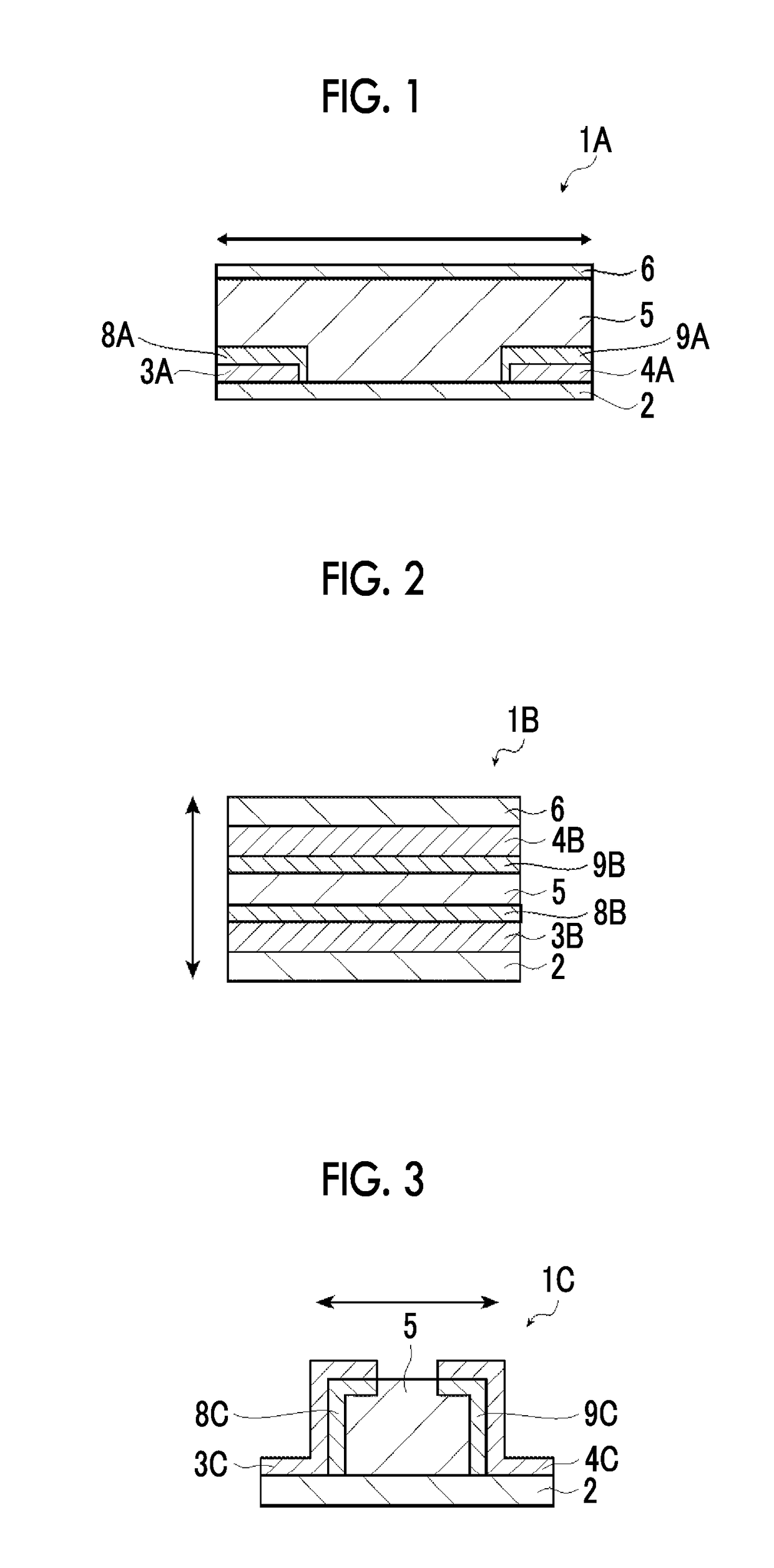
[0047]FIG. 1 is a view conceptually showing a thermoelectric conversion element of a first embodiment that is an example of the thermoelectric conversion element of the present invention.

[0048]As shown in FIG. 1, a thermoelectric conversion element 1A has a substrate 2, a first electrode 3A and a second electrode 4A disposed on the substrate 2 at positions spaced apart from each other, a first buffer layer 8A disposed to come into contact with the first electrode 3A on the substrate 2, a second buffer layer 9A disposed to come into contact with the second electrode 4A on the substrate 2, a thermoelectric conversion layer 5 disposed to come into contact with the first buffer layer 8A and the second buffer layer 9A on the substrate 2, and a protective substrate 6 disposed on the thermoelectric conversion layer 5. At the time of using the thermoelectric conversion element 1A, as shown in FIG. 1, a temperature difference is caused in the direction of the arrow.

[0049]As shown in FIG. 1, ...

second embodiment

[0165]FIG. 2 is a view conceptually showing a thermoelectric conversion element of a second embodiment that is an example of the thermoelectric conversion element of the present invention.

[0166]As shown in FIG. 2, a thermoelectric conversion element 1B is an element having a substrate 2, a first electrode 3B, a first buffer layer 8B, a thermoelectric conversion layer 5, a second buffer layer 9B, a second electrode 4B, and a protective substrate 6 in this order. The thermoelectric conversion element 1B shown in FIG. 2 is an aspect in which an electromotive force (voltage) is obtained using a temperature difference caused in the direction indicated by the arrow.

[0167]As shown in FIG. 2, each of the first buffer layer 8B and the second buffer layer 9B is disposed between the thermoelectric conversion layer 5 and the electrode (the first electrode 3B and the second electrode 4B) and electrically connects the thermoelectric conversion layer 5 and the electrode to each other. That is, eac...

third embodiment

[0170]FIG. 3 is a view conceptually showing a thermoelectric conversion element of a third embodiment that is an example of the thermoelectric conversion element of the present invention.

[0171]As shown in FIG. 3, a thermoelectric conversion element 1C has a substrate 2, a thermoelectric conversion layer 5 disposed on the substrate 2, a first buffer layer 8C disposed on a portion of the top surface and one lateral surface of the thermoelectric conversion layer 5, a second buffer layer 9C disposed on a portion of the top surface and the other lateral surface of the thermoelectric conversion layer 5, a first electrode 3C disposed on the top surface and a lateral surface of the first buffer layer 8C, and a second electrode 4C disposed on the top surface and a lateral surface of the second buffer layer 9C. The thermoelectric conversion element 1C shown in FIG. 3 is an aspect in which an electromotive force (voltage) is obtained by using a temperature difference caused in the direction in...


PUM

PropertyMeasurementUnit
pKaaaaaaaaaaa
oxidation-reduction potentialaaaaaaaaaa
thermoelectricaaaaaaaaaa

Abstract

An object of the present invention is to provide a thermoelectric conversion element having excellent thermoelectric conversion performance and excellent high-temperature durability, a method for manufacturing the thermoelectric conversion element, a thermoelectric conversion module, and a method for manufacturing the thermoelectric conversion module. A thermoelectric conversion element of the present invention has a thermoelectric conversion layer containing an organic thermoelectric conversion material and a dopant, a pair of electrodes disposed at positions separated from each other, and a buffer layer which is disposed between the thermoelectric conversion layer and each of the electrodes and electrically connects the thermoelectric conversion layer and the electrodes to each other, in which the buffer layer contains the same material as the organic thermoelectric conversion material contained in the thermoelectric conversion layer, the buffer layer does not contain a dopant or contains a dopant, and in a case where the buffer layer contains a dopant, a ratio of the dopant contained in the buffer layer to the dopant contained in the thermoelectric conversion layer is equal to or lower than 0.1.

Description

CROSS-REFERENCE TO RELATED APPLICATIONS[0001]This application is a Continuation of PCT International Application No. PCT / JP2017 / 008731 filed on Mar. 6, 2017, which claims priority under 35 U.S.C. § 119(a) to Japanese Patent Application No. 2016-045481 filed on Mar. 9, 2016. The above application is hereby expressly incorporated by reference, in its entirety, into the present application.BACKGROUND OF THE INVENTION1. Field of the Invention[0002]The present invention relates to a thermoelectric conversion element, a method for manufacturing a thermoelectric conversion element, a thermoelectric conversion module, and a method for manufacturing a thermoelectric conversion module.2. Description of the Related Art[0003]Thermoelectric conversion materials that enable the interconversion of thermal energy and electric energy are used in thermoelectric generation elements or thermoelectric conversion elements such as a Peltier element. Thermoelectric generation using the thermoelectric conve...

Claims


Application Information

Patent Timeline
Patent Type & Authority Applications(United States)
IPC IPC(8): H01L35/08H01L35/24H01L35/32H01L35/34H01L51/00
CPCH01L35/08H01L35/24H01L35/32H01L35/34H01L51/0048H01L51/005H01L51/004H01L51/0036H01L51/0093B82Y30/00H10N10/817H10N10/856H10N10/17B82Y40/00H10K85/60H10K85/113H10K85/141H10K85/221H10K85/761H10N10/01H10N10/857
Inventor SUGIURA, HIROKIKANAZAWA, YOSHINORIHAYASHI, NAOYUKINOMURA, KIMIATSU
Owner FUJIFILM CORP
Why Eureka
Try Eureka