Semiconductor package device and method of manufacturing the same

Active Publication Date: 2019-01-10
ADVANCED SEMICON ENG INC
View PDF5 Cites 1 Cited by
  • Summary
  • Abstract
  • Description
  • Claims
  • Application Information

AI Technical Summary

Benefits of technology

[0003]In one or more embodiments, an image sensor comprises a chip, a first redistribution layer (RDL), a second RDL and a third RDL. The chip has a first surface, a second surface opposite to the first surface and a lateral surface extending between the first surface and the second surface. The first RDL is disposed on the first surface of the chip and extends along the first surface of the chip and beyond the lateral surface of the chip. The second RDL is disposed on the second surface of the chip. The third RDL is disposed on the lateral surface of the chip and connects the first RDL to the second RDL.
[0004]In one or more embodiments, an image sensor comprises a substrate, a micro-lens array, a first RDL and a second RDL. The substrate has a first surface, a second surface opposite to the first surface and a lateral surface extending between the first surface and the second surface. The micro-lens array is disposed on the first surface of the substrate. The first RDL is disposed on the first surface of the substrate an

Problems solved by technology

However, the use of the TSV would increa

Method used


Image

  • Semiconductor package device and method of manufacturing the same
  • Semiconductor package device and method of manufacturing the same
  • Semiconductor package device and method of manufacturing the same

Examples


Embodiment Construction

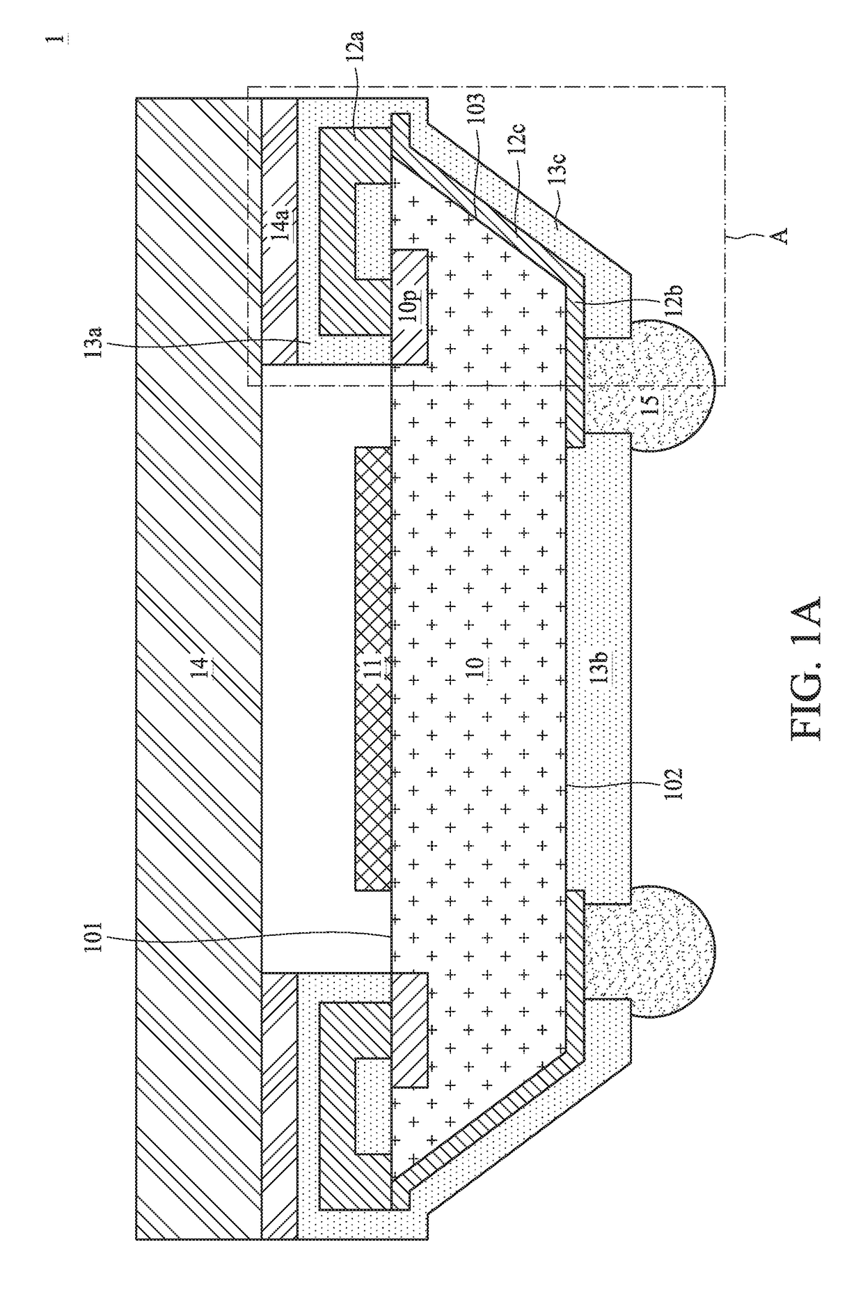
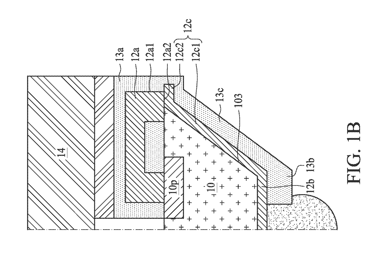
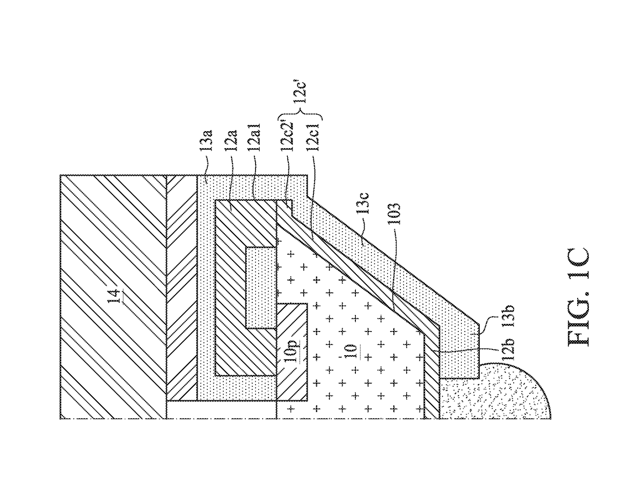
[0015]FIG. 1A illustrates a cross-sectional view of a semiconductor package device 1 in accordance with some embodiments of the present disclosure. The semiconductor package device 1 includes a chip (or a die) 10, conductive layers 12a, 12b, 12c, dielectric layers 13a, 13b, 13c, a cover 14, and one or more electrical contacts 15.

[0016]The chip 10 has an active surface 101 (also referred to as a “first surface”), a back surface 102 (also referred to as a “second surface”) opposite to the active surface 101 and a lateral surface 103 extending between the active surface 101 and the back surface 102. In some embodiments, the lateral surface 103 is not perpendicular to the active surface 101 or the back surface 102. For example, an angle defined by the active surface 101 and the lateral surface 103 may be an acute angle less than about 90 degrees while an angle defined by the back surface 102 and the lateral surface 103 may be an obtuse angle greater than about 90 degrees. In some other ...


PUM


Abstract

An image sensor comprises a chip, a first redistribution layer (RDL), a second RDL and a third RDL. The chip has a first surface, a second surface opposite to the first surface and a lateral surface extending between the first surface and the second surface. The first RDL is disposed on the first surface of the chip and extends along the first surface of the chip and beyond the lateral surface of the chip. The second RDL is disposed on the second surface of the chip. The third RDL is disposed on the lateral surface of the chip and connects the first RDL to the second RDL.

Description

BACKGROUND1. Technical Field[0001]The present disclosure relates generally to a semiconductor package device and a method of manufacturing the same. More particularly, the present disclosure relates to a semiconductor package device including an image sensor and a method of manufacturing the same.2. Description of the Related Art[0002]In a Complementary Metal-Oxide-Semiconductor (CMOS) image sensor, an active side and a back side of the image sensor can be electrically connected by a through silicon via (TSV). However, the use of the TSV would increase the manufacturing cost and complexity.SUMMARY[0003]In one or more embodiments, an image sensor comprises a chip, a first redistribution layer (RDL), a second RDL and a third RDL. The chip has a first surface, a second surface opposite to the first surface and a lateral surface extending between the first surface and the second surface. The first RDL is disposed on the first surface of the chip and extends along the first surface of th...

Claims


Application Information

Patent Timeline
IPC IPC(8): H01L27/146
CPCH01L27/14636H01L27/14643H01L27/14627H01L27/14618H01L27/14685H01L27/14689H01L27/14687
Inventor TSENG, CHI SHENG
Owner ADVANCED SEMICON ENG INC
Why Eureka
Try Eureka