Apparatus for fabricating a semiconductor device

Active Publication Date: 2006-07-18
NTT MOBILE COMM NETWORK INC
View PDF14 Cites 17 Cited by
  • Summary
  • Abstract
  • Description
  • Claims
  • Application Information

AI Technical Summary

Benefits of technology

[0013]In the present invention, a ring-shaped holder for mounting a wafer thereon is inserted and maintained in the grooves formed in the supporting bars of a boat. Thus, such holder provides greater contact area compared to the conventional method of directly loading the wafers into the grooves. Naturally, the adverse effects of using the conventional method of direct loading are effectively eliminated.
[0014]In other words, during the heat treatment process performed at varying temperatures throughout the process, the wafer experiences deformations due to, e.g., temperature variations during wafer temperature ramping up and down processes and a high heat treatment temperature; and i

Problems solved by technology

Such minimal surface contact generates augmented deformation (due to the weight of the wafer itself) and thermal stresses in the wafers, producing defects, e.g., slip, therein.
Further, if the grooves have sharp edges contacting the heated wafers, such local contacts can easily produce scratches on the wafers softened by heat.
Moreover, the situa

Method used


Image

  • Apparatus for fabricating a semiconductor device
  • Apparatus for fabricating a semiconductor device
  • Apparatus for fabricating a semiconductor device

Examples


Example

[0027]Hereinafter, a first preferred embodiment of the present invention will be described with reference to the accompanying drawings of FIGS. 1 to 3D.

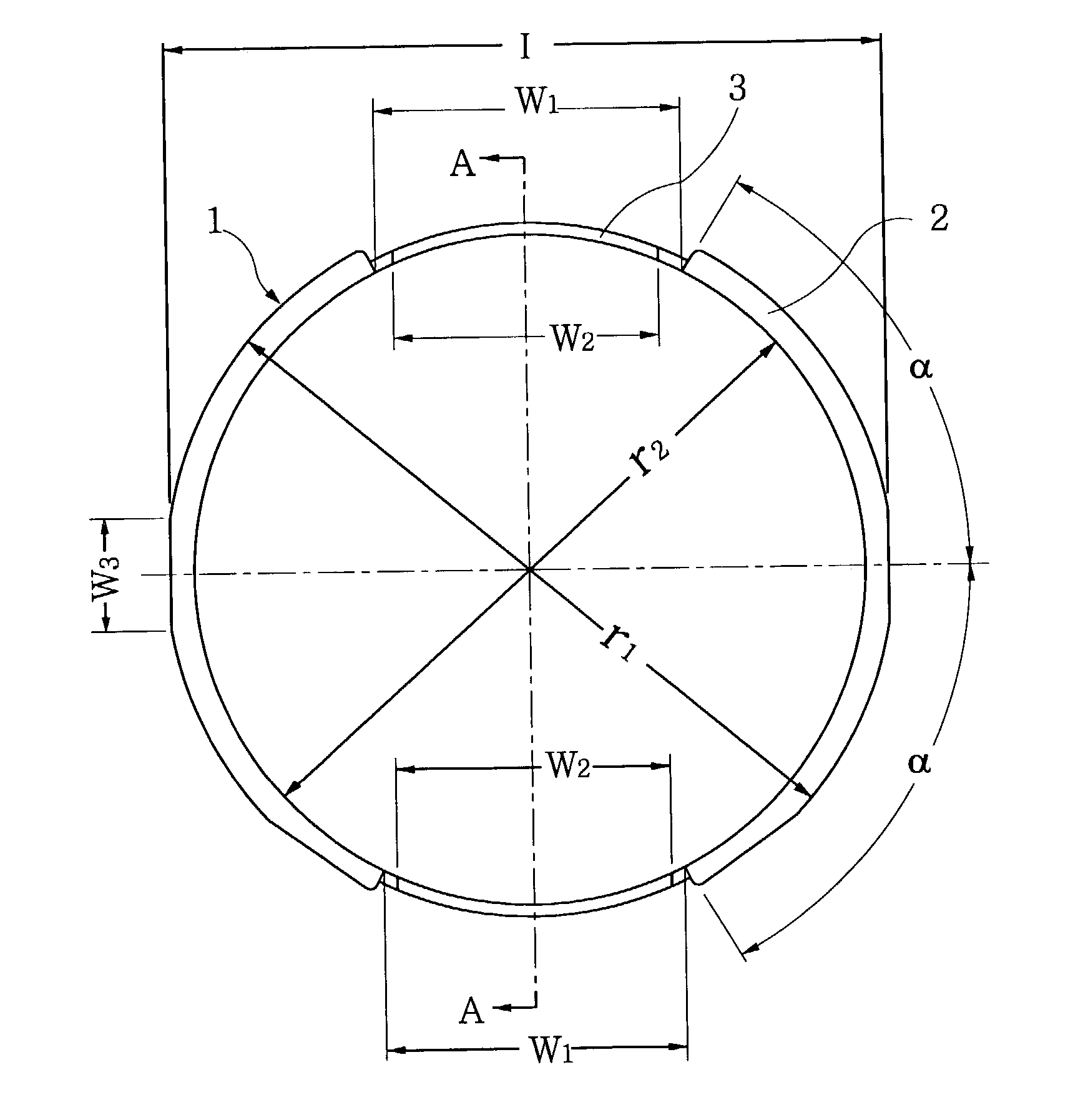
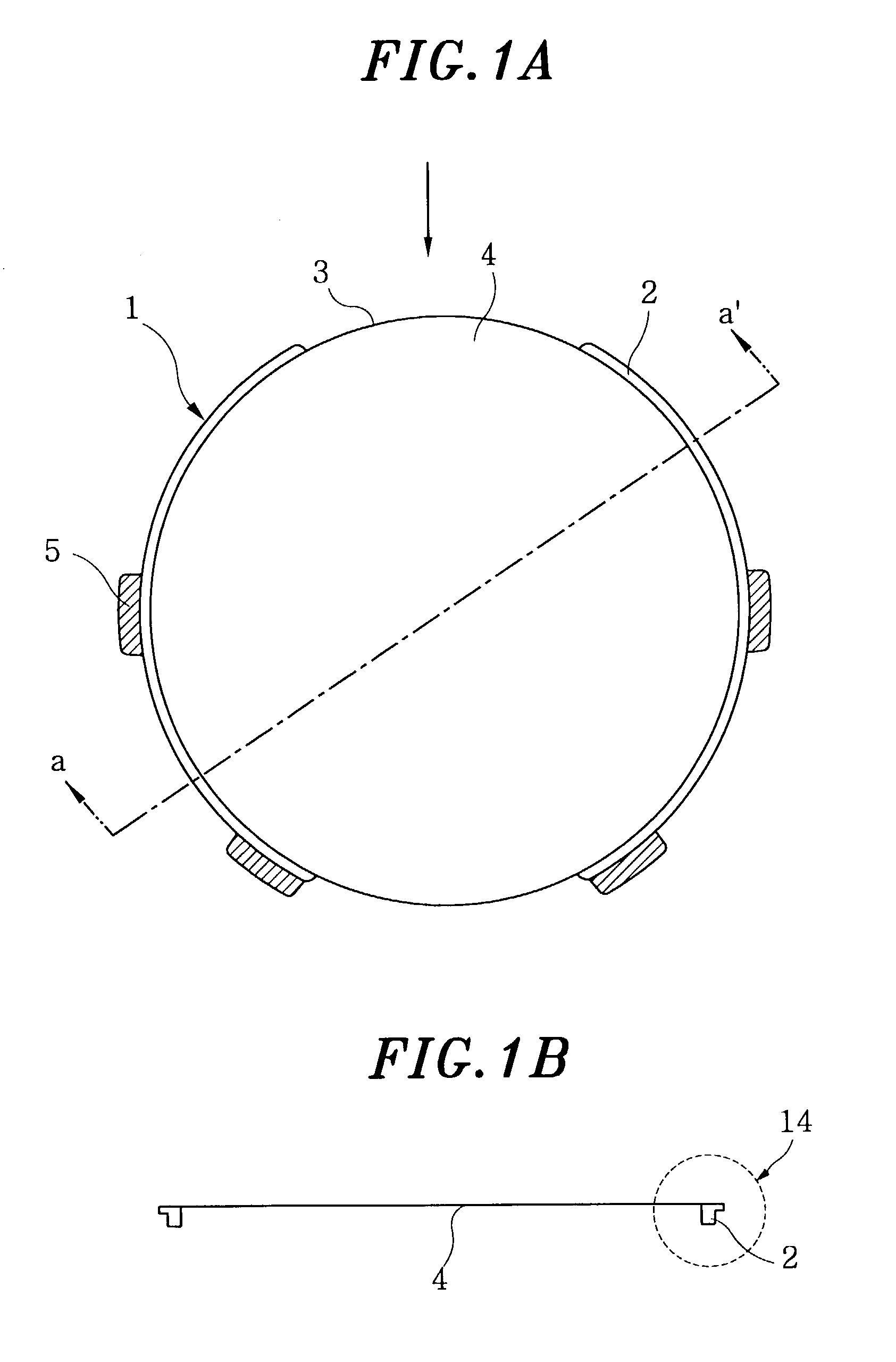
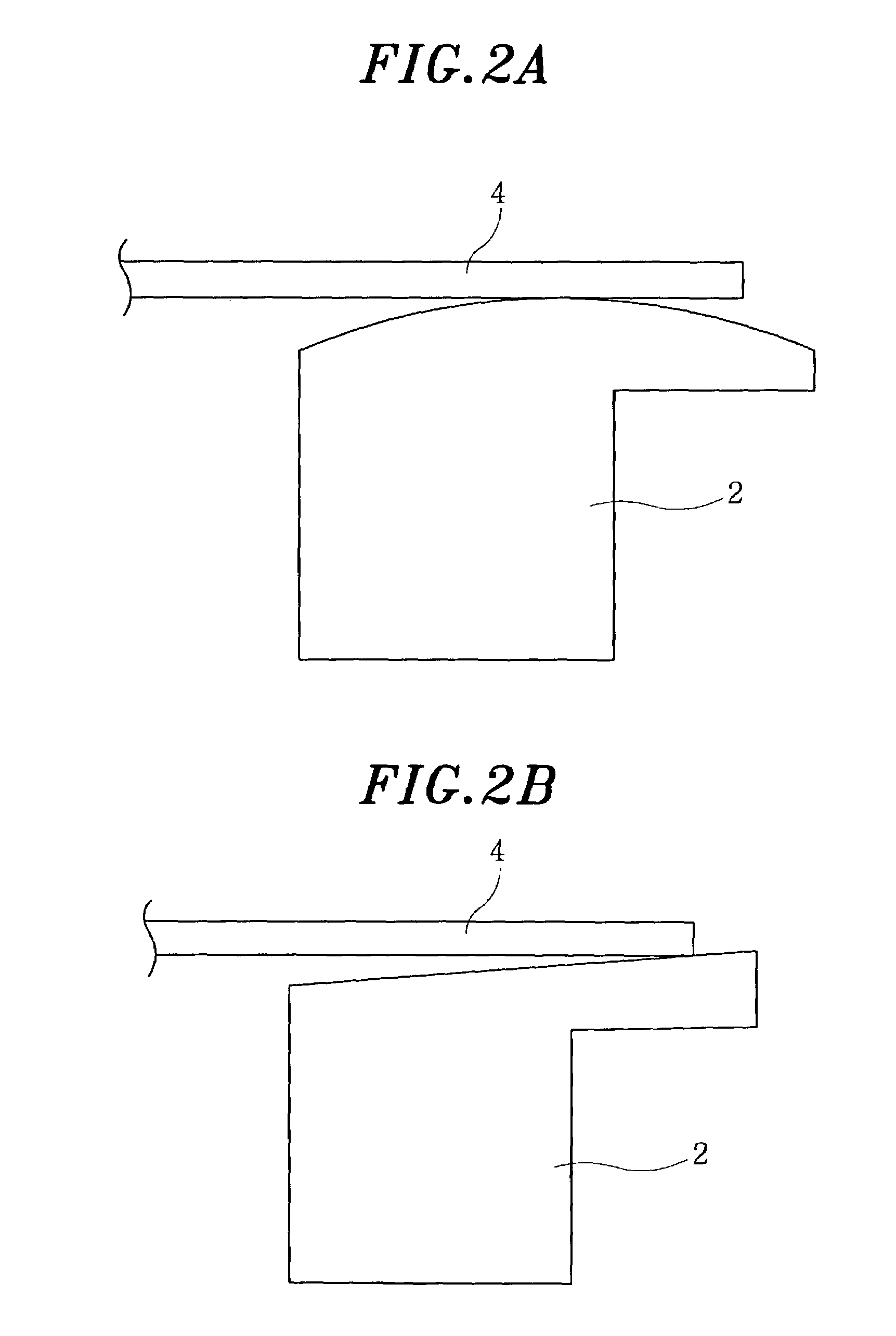
[0028]FIG. 3A shows a plan view of a holder 1 in accordance with the first preferred embodiment of the present invention; FIG. 3B describes a front view of the holder 1 of FIG. 3A; FIG. 3C illustrates an enlarged view of a portion “D” shown in FIG. 3B; and FIG. 3D presents a partial cross sectional view of the holder taken along the line A—A shown in FIG. 3A.

[0029]As shown in FIG. 3A, the holder 1 for mounting a wafer or substrate 4 thereon and formed in a shape of ring includes brims (thicker portions) 2 and recessed portions (thinner portions) 3 having upper surfaces lower than those of the brims 2. The holder 1 has a generally flat bottom surface. The ring-shaped holder 1, as shown in FIG. 1A, is inserted into grooves formed in the boat supporting bars 5 provided in a boat to be supported thereby. A wafer 4 to be processed is disp...


PUM

PropertyMeasurementUnit
Widthaaaaaaaaaa
Heightaaaaaaaaaa
Circumferenceaaaaaaaaaa

Abstract

A semiconductor fabricating apparatus having a structure, which facilitates a loading and unloading operation of wafers while having a low effect by a high temperature during a heat treatment. The semiconductor fabricating apparatus includes a plurality of ring-shaped holder having brims and recessed portions, the brims for mounting the to-be-processed wafers thereon, thereby performing the required heat treatment. A tweezer plate of a wafer loading-transferring device is inserted onto the recessed portion or taken out therefrom, and the inserted tweezer plate is ascended or descended, so that the wafer can be inserted on the brims or taken out therefrom.

Description

FIELD OF THE INVENTION[0001]The present invention relates to an apparatus for fabricating a semiconductor device; and, more particularly, to an apparatus capable of efficiently performing various heat treatments and facilitating transferring of a wafer onto / from a holder, while preventing slip and generation of impurities and scratches on the wafer.BACKGROUND OF THE INVENTION[0002]In fabricating semiconductor devices, various heat treatments such as an oxidation treatment, a diffusion process, a chemical vapor deposition (CVD) process or the like are performed. A vertical type heat treatment apparatus having a boat with a plurality of wafers vertically stacked therein is used in performing such heat treatments.[0003]The wafers are first vertically stacked at a predetermined interval inside the boat, and the boat is then loaded into a reaction chamber. Thereafter, the vertically stacked wafers are heat-treated using a heating unit while supplying into the reaction chamber gas chosen ...

Claims


Application Information

Patent Timeline
IPC IPC(8): H01L21/00C23C16/00C23C16/458H01L21/673H01L21/687
CPCC23C16/4583H01L21/67109H01L21/68707H01L21/67309Y10S206/832H01L21/02
Inventor SHIMADA, TOMOHARU
Owner NTT MOBILE COMM NETWORK INC
Why Eureka
Try Eureka