Array substrate, manufacturing method thereof, and display device

a technology of array substrate and manufacturing method, applied in the field of array substrate, can solve problems such as parametric capacitance generation, and achieve the effects of reducing the signal delay on improving charging rate and display effect, and reducing the delay of scan line and/or data lin

Active Publication Date: 2019-01-24
SHENZHEN CHINA STAR OPTOELECTRONICS SEMICON DISPLAY TECH CO LTD
View PDF1 Cites 1 Cited by
  • Summary
  • Abstract
  • Description
  • Claims
  • Application Information

AI Technical Summary

Benefits of technology

[0016]By disposing at least an auxiliary segment corresponding to each scan line and/or each data line on the array substra...

Problems solved by technology

In the mean time, because the scan lines and data lines of the LCD device overlap much, parasitic capacitance is generated du...

Method used


Image

  • Array substrate, manufacturing method thereof, and display device
  • Array substrate, manufacturing method thereof, and display device
  • Array substrate, manufacturing method thereof, and display device

Examples


Embodiment Construction

[0027]To further explain the technical means and effect of the present invention, the following refers to embodiments and drawings for detailed description. Apparently, the described embodiments are merely some embodiments of the present invention, instead of all embodiments. All other embodiments based on embodiments in the present invention and obtained by those skilled in the art without departing from the creative work of the present invention are within the scope of the present invention.

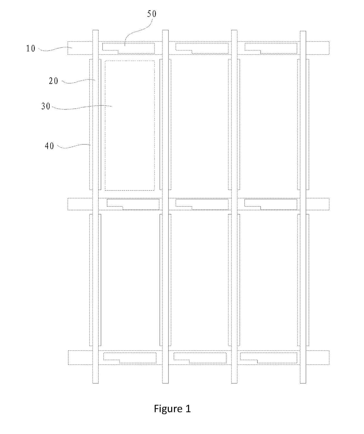
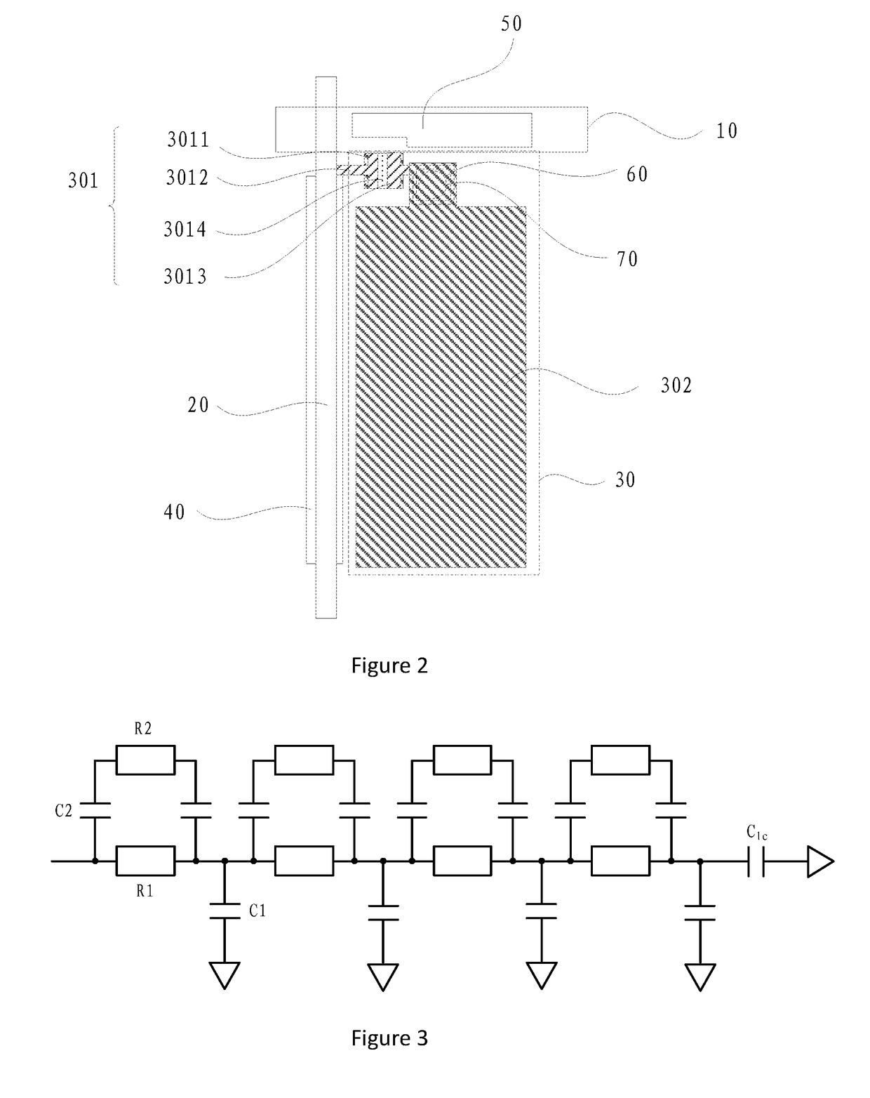
[0028]Refer to FIG. 1 and FIG. 2. An array substrate of the present invention comprises:

[0029]a plurality of scan lines 10;

[0030]a plurality of data lines 20, intersecting with the plurality of scan lines 10 so as to define a plurality of pixel areas 30;

[0031]a plurality of auxiliary segments, wherein each of the plurality of scan lines 10 and / or each of the plurality of data lines 20 corresponding respectively to at least an auxiliary segment, the scan lines 10 and / or data lines 20 forming cap...


PUM


Abstract

An array substrate, manufacturing method thereof and display device are provided. The array substrate includes a plurality of scan lines, a plurality of data lines intersecting with the plurality of scan lines to as to define a plurality of pixel areas; a plurality of auxiliary segments, and each scan line and/or each data line respectively corresponding to at least a auxiliary segment, the scan line and/or data line and the corresponding auxiliary segment forming capacitive coupling to reduce signal delay on the scan line and/or data line. As such, the signal delay on the scan line and/or data line is reduced, and the charging rate and display effect are improved.

Description

BACKGROUND OF THE INVENTION1. Field of the Invention[0001]The present invention relates to the field of display techniques, and in particular to an array substrate, manufacturing method thereof, and display device.2. The Related Arts[0002]The liquid crystal display (LCD), due to the advantages of light-weight, small-size and low power-consumption, has become the most widely used panel display device, and applied to cell phones, digital cameras, PC, and other electronic devices.[0003]As the resolution of LCD device increases and the pixel charging time decreases, the pixel charging rate decreases because the loading of the pixel is unchanged. In the mean time, because the scan lines and data lines of the LCD device overlap much, parasitic capacitance is generated during charging, which becomes the main factor in signal delay when combined with the resistance of the scan line and the date lines. As such, the pixel charging rate is affected, and the display effect of the LCD is reduced...

Claims


Application Information

Patent Timeline
IPC IPC(8): G02F1/1362G02F1/1368H01L27/12G02F1/1335
CPCG02F1/136286G02F1/1368H01L27/124H01L27/1262G02F1/136227G02F1/133516G02F2201/122G02F2001/136295G02F2001/136222G02F1/136272G02F1/136222G02F1/136295
Inventor HAO, SIKUN
Owner SHENZHEN CHINA STAR OPTOELECTRONICS SEMICON DISPLAY TECH CO LTD
Why Eureka
Try Eureka