
Three-dimensional semiconductor memory device

Active Publication Date: 2019-01-31
SAMSUNG ELECTRONICS CO LTD
View PDF20 Cites 12 Cited by
  • Summary
  • Abstract
  • Description
  • Claims
  • Application Information

AI Technical Summary

Benefits of technology

This patent describes a new type of memory that can store data in three dimensions, making it more reliable and dense than previous options.

Problems solved by technology

However, the extremely expensive process equipment needed to increase pattern fineness sets a practical limitation on increasing integration for two-dimensional or planar semiconductor devices.

Method used


Image

  • Three-dimensional semiconductor memory device
  • Three-dimensional semiconductor memory device
  • Three-dimensional semiconductor memory device

Examples


Embodiment Construction

[0030]Some example embodiments of the inventive concept will now be described more fully with reference to the accompanying drawings.

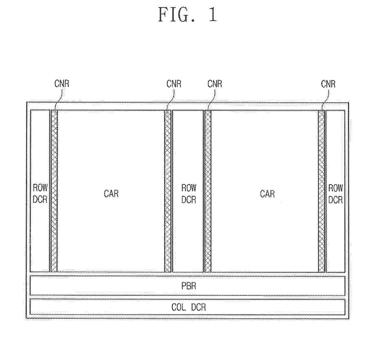
[0031]FIG. 1 is a plan view illustrating a schematic configuration of a three-dimensional semiconductor memory device according to some embodiments of the inventive concept.

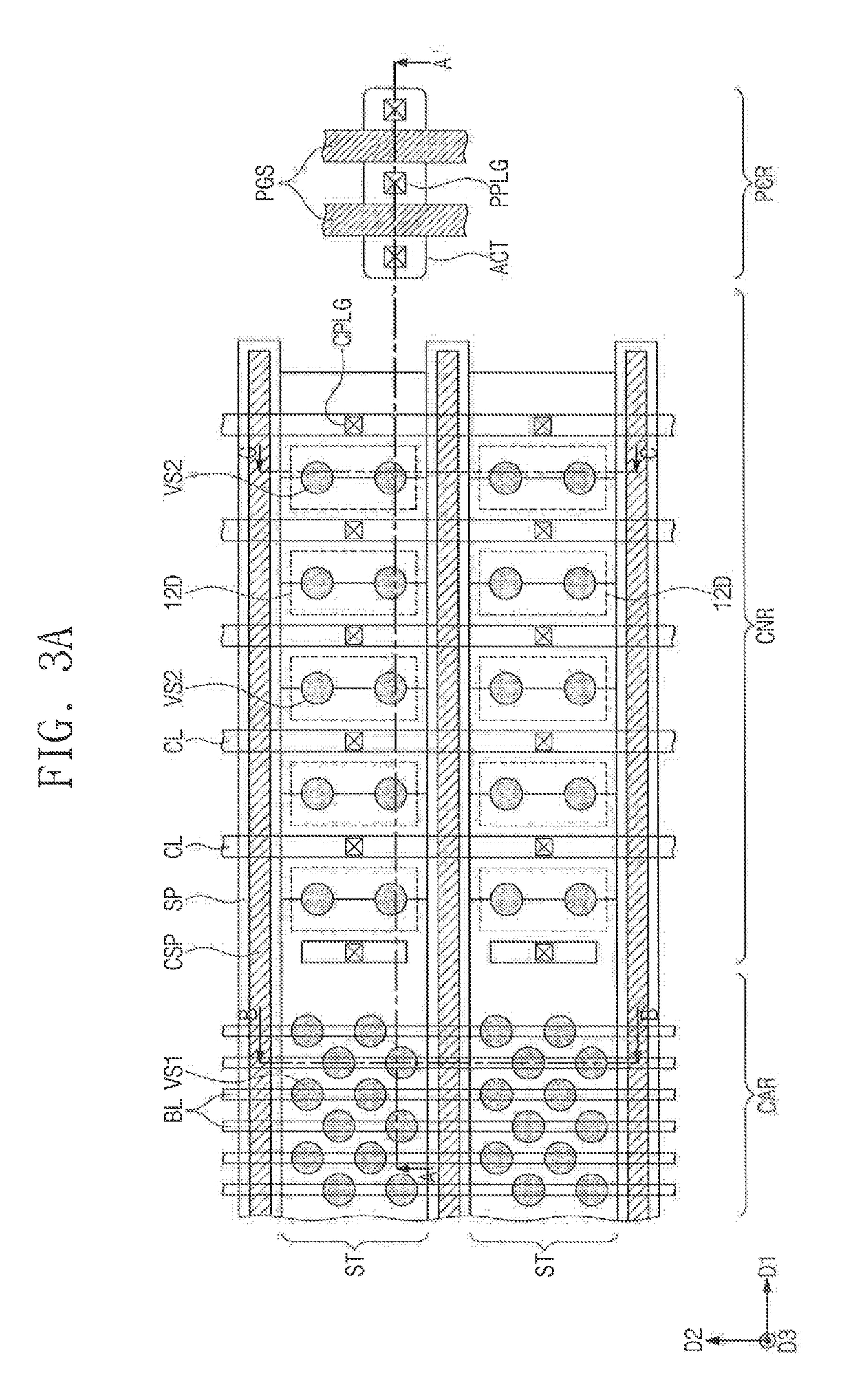
[0032]Referring now to FIG. 1, a three-dimensional semiconductor memory device may include a cell array region CAR and a peripheral circuit region PCR. The peripheral circuit region may include row decoder regions ROW DCR, a page buffer region PBR, a column decoder region COL, DCR, and a control circuit region (not shown). In some embodiments of the inventive concept, a connection region CNR may be provided between the cell array region CAR and each of the row decoder regions ROW DCR.

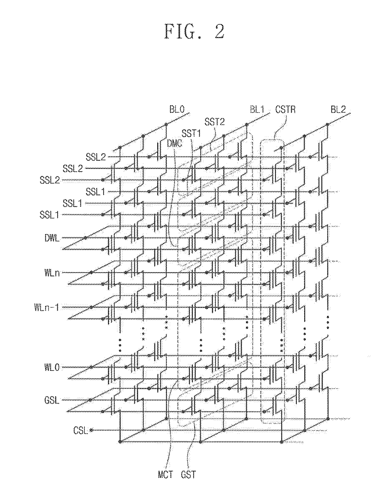
[0033]A memory cell array including a plurality of memory cells may be provided in the cell array region CAR. In some embodiments of the inventive concept, the memory cell array may include a plurality ...


PUM


Abstract

A three-dimensional semiconductor memory device and a method of manufacturing the same. The device may include a substrate including a cell array region and a connection region, an electrode structure including electrodes vertically stacked on the substrate, a plurality of first vertical structures penetrating the electrode structures on the cell array region, and a plurality of second vertical structures penetrating the electrode structures on the connection region. Each of the first and second vertical structures may include a lower semiconductor pattern connected to the substrate and an upper semiconductor pattern connected to the lower semiconductor pattern.

Description

CROSS-REFERENCE TO RELATED APPLICATIONS[0001]This U.S. non-provisional patent application claims priority under 35 U.S.C. § 11.9 to Korean Patent Application No. 10-2017-0094401, filed on Jul. 25, 2017, in the Korean Intellectual. Property Office, the entire contents of which are incorporated by reference herein.1. TECHNICAL FIELD[0002]The inventive concept relates to a three-dimensional semiconductor memory device, and in particular, to a three-dimensional semiconductor memory device with high reliability and a high integration density.2. DISCUSSION OF THE RELATED ART[0003]Higher integration of semiconductor devices may lead to satisfying consumer demands for superior performance of electronic devices having relatively inexpensive prices. In the case of semiconductor devices, higher integration is an important factor in determining product prices, thus such advancements are desirable. In the case of conventional two-dimensional or planar semiconductor devices, their integration is ...

Claims


Application Information

Patent Timeline
IPC IPC(8): H01L27/11582H01L27/11556H01L27/11526H01L27/11573H01L29/792
CPCH01L27/11582H01L27/11556H01L27/11526H01L27/11573H01L29/7926H10B41/35H10B41/20H10B43/50H10B43/40H10B43/27H10B43/35H10B43/20H10B41/27H10B41/40H10B41/50
Inventor KIM, JONGWONJUNG, YOUNG-JIN
Owner SAMSUNG ELECTRONICS CO LTD
Features
  • Generate Ideas
  • Intellectual Property
  • Life Sciences
  • Materials
  • Tech Scout
  • Unparalleled Data Quality
  • Higher Quality Content
  • 60% Fewer Hallucinations
Learn More