
Systems and methods for high energy x-ray detection in electron microscopes

a high-energy x-ray and electron microscope technology, applied in the field of systems and methods for high-energy x-ray detection in electron microscopes, can solve the problems of low-resolution spectra and/or poor statistical quality of elemental identification

Active Publication Date: 2019-02-07
EDAX
View PDF6 Cites 15 Cited by
  • Summary
  • Abstract
  • Description
  • Claims
  • Application Information

AI Technical Summary

Benefits of technology

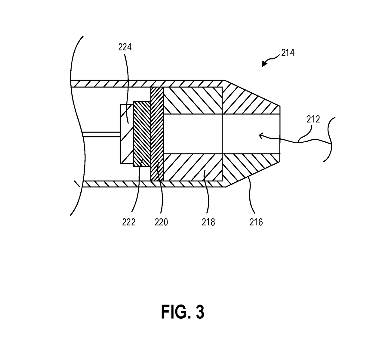
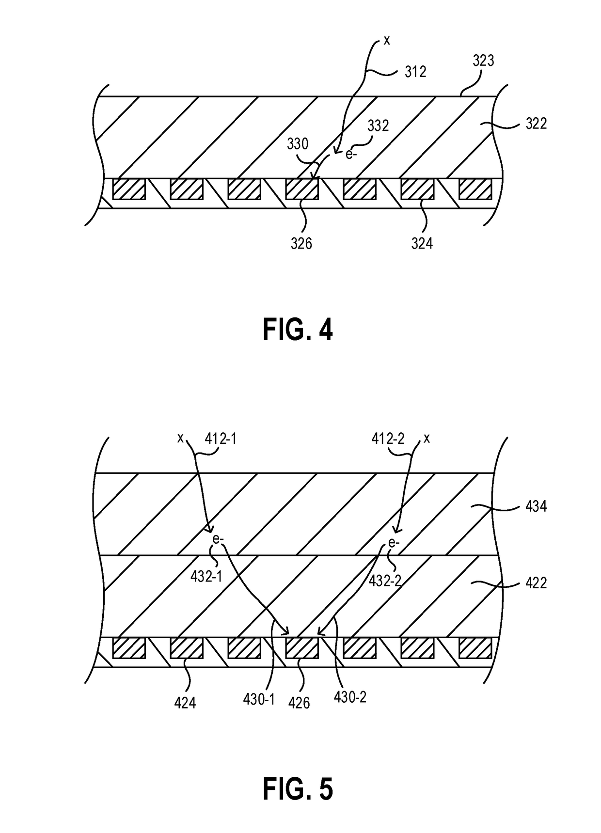
The patent describes a system for collecting information from a sample using an X-ray detector. The detector has a detection tip with a layer of compound semiconductor material. This material can be a binary compound semiconductor or a silicon-based semiconductor material layered with the compound semiconductor. The technical effects of this system include improved detection and analysis of samples using X-ray based methods.

Problems solved by technology

The relatively low X-ray counts result in low-resolution spectra and / or poor statistical quality of the elemental identification.

Method used


Image

  • Systems and methods for high energy x-ray detection in electron microscopes
  • Systems and methods for high energy x-ray detection in electron microscopes
  • Systems and methods for high energy x-ray detection in electron microscopes

Examples


Embodiment Construction

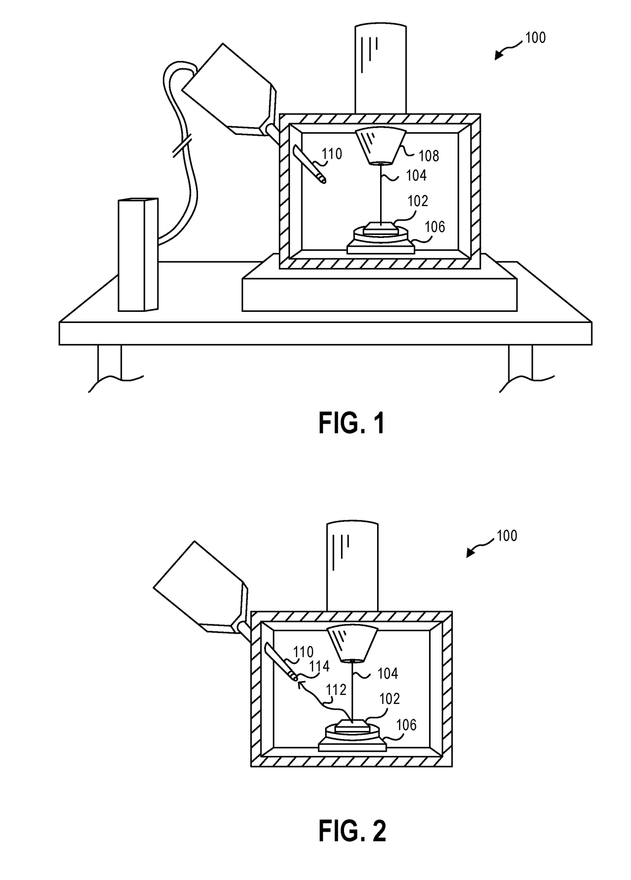
[0020]This disclosure generally relates to data collection devices, systems, and methods for collecting information from a sample. More specifically, the present disclosure relates to improved collection and detection of X-rays emitted from a sample excited by an excitation source. In some embodiments, the excitation source may be an electron source, such as a field emission, LaB6, tungsten, or other filament source. The electron source may emit electrons that are then accelerated toward the sample. The electron beam may be focused, collimated, and directed by a plurality of magnets to position the electron source on the surface of the sample and impart energy onto the surface. While one or more examples may specifically describe a scanning electron microscope, it should be understood that a detector and a detection material according to the present disclosure may be applicable to any electron microscope, such as a high-pressure electron microscope, a transmission electron microscop...


PUM


Abstract

A system for collecting information from a sample, the system includes an X-ray detector configured to mount to an electron microscope, the X-ray detector including a detection tip with a detection material positioned in the detection tip. The detection material includes a compound semiconductor material.

Description

CROSS-REFERENCE TO RELATED APPLICATIONS[0001]This application claims the benefit of U.S. Provisional Patent Application No. 62 / 541,226, filed on Aug. 4, 2017, which are hereby incorporated by reference in their entireties.BACKGROUND OF THE DISCLOSURE[0002]Data collection systems are used for material analysis and microanalysis of a variety of material properties including chemical, structural, mechanical, crystallographic, or other information. For example, Energy Dispersive Spectrometry (“EDS”) has grown into a robust analytic technique for the measurement of material properties. EDS is an analytical technique performed in a scanning electron microscope (“SEM”) or transmission electron microscope (“TEM”) in a low pressure or near vacuum environment. A sample is positioned beneath a column housing an electron source. The electron source may be any suitable source, such as a tungsten filament, thermal field emission, or LaB6 electron source. The electron source may emit electrons tha...

Claims


Application Information

Patent Timeline
Patent Type & Authority Applications(United States)
IPC IPC(8): H01J37/244H01J37/28
CPCH01J37/244H01J37/28H01J2237/2802H01J2237/2442H01J2237/24475H01J2237/28
Inventor CAMUS, PATRICK PAUL
Owner EDAX
Learn More