
Semiconductor device, photoelectronic device, and method for manufacturing transistion-metal dichalcogenide thin film

Active Publication Date: 2019-02-07
RES & BUSINESS FOUNDATION SUNGKYUNKWAN UNIV
View PDF2 Cites 5 Cited by
  • Summary
  • Abstract
  • Description
  • Claims
  • Application Information

AI Technical Summary

Benefits of technology

The present patent describes a way to create a thin film made of transition-metal dichalcogenide that has different numbers of layers. This results in different band gaps and electron affinity between the layers, which leads to high photocurrent and improved optical properties, such as photoresponsivity. This thin film can be used to create various functional devices with excellent electrical and optical properties, including semiconductor devices and photoelectronic devices.

Problems solved by technology

However, in the case of performing the above-described separation in the same manner as mechanical peeling, such as using a adhesive tape, it is almost impossible to form TMD-based multiple junctions.
Thus, there is a problem that a hetero-junction may not be formed to have the target number and pattern of the layers.

Method used


Image

  • Semiconductor device, photoelectronic device, and method for manufacturing transistion-metal dichalcogenide thin film
  • Semiconductor device, photoelectronic device, and method for manufacturing transistion-metal dichalcogenide thin film
  • Semiconductor device, photoelectronic device, and method for manufacturing transistion-metal dichalcogenide thin film

Examples


Embodiment Construction

[0028]Examples of various embodiments are illustrated and described further below. It will be understood that the description herein is not intended to limit the claims to the specific embodiments described. On the contrary, it is intended to cover alternatives, modifications, and equivalents as may be included within the spirit and scope of the present disclosure as defined by the appended claims.

[0029]The same reference numbers in different figures. denote the same or similar elements, and as such perform similar functionality. Further, descriptions and details of well-known steps and elements are omitted for simplicity of the description. Furthermore, in the following detailed description of the present disclosure, numerous specific details are set forth in order to provide a thorough understanding of the present disclosure. However, it will be understood that the present disclosure may be practiced without these specific details. In other instances, well-known methods, procedure...


PUM


Abstract

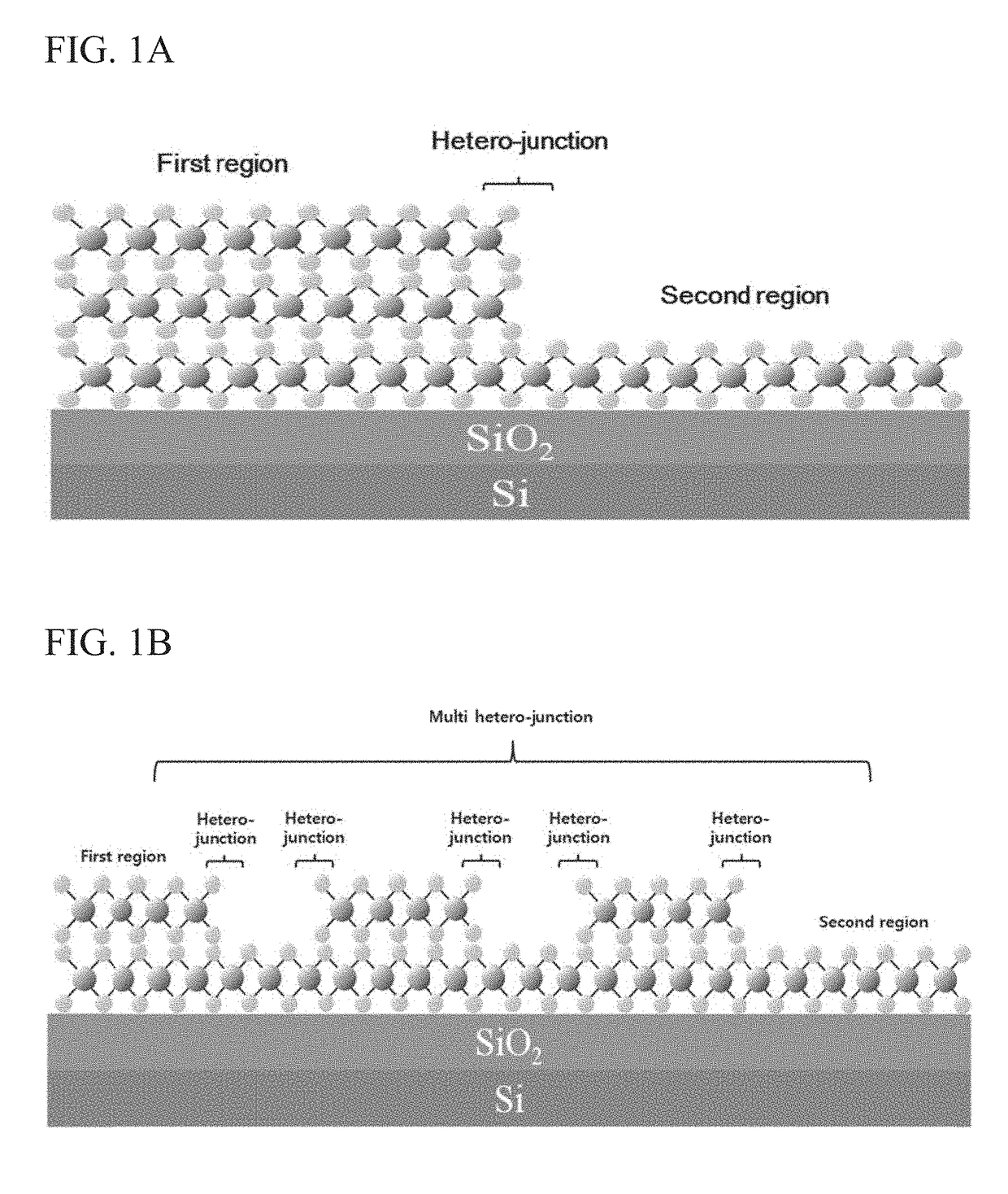
The present disclosure relates to a semiconductor device and a photoelectronic device, both including a transition-metal dichalcogenide thin-film, and to a method for producing a transition-metal dichalcogenide thin-film. The transition-metal dichalcogenide thin-film includes: a first region including a stack of N+M transition-metal dichalcogenide molecular layers; and a second region including a stack of N transition-metal dichalcogenide molecular layers, wherein the second region is horizontally adjacent to the first region, wherein the N transition-metal dichalcogenide molecular layers of the second region respectively horizontally extend from the N transition-metal dichalcogenide molecular layers of the first region.

Description

CROSS-REFERENCE TO RELATED APPLICATIONS[0001]This application claims the priority of Korean Patent Application No. 10-2017-0097527 filed on Aug. 1, 2017, in the Korean Intellectual Property Office, the disclosure of which is hereby incorporated by reference in its entirety.BACKGROUND1. Technical Field[0002]The present disclosure relates to a semiconductor device, a photoelectronic device, and to a method for manufacturing a transition-metal dichalcogenide thin-film. More particularly, the present disclosure relates to a semiconductor device and a photoelectronic device, both including a transition-metal dichalcogenide thin-film, and to a method for producing a transition-metal dichalcogenide thin-film.2. Description of the Related Art[0003]Transition-metal dichalcogenides (TMDs) are compounds includng a bond between a transition-metal atom (M) and a chalcogen atom (X). The TMD compound defines a two-dimensional material with a layered structure in which molecular layers is combined ...

Claims


Application Information

Patent Timeline
IPC IPC(8): H01L31/0392H01L31/032H01L31/0352H01L31/18
CPCH01L31/0392H01L31/0324H01L31/035272H01L31/18H01L31/112Y02E10/50H01L31/032H01L31/072H01L31/10Y02P70/50
Inventor YEOM, GEUN YOUNGKIM, KI SEOKKIM, KI HYUNPARK, JIN WOOKIM, DOO SANJI, YOU JINBYUN, JI YOUNG
Owner RES & BUSINESS FOUNDATION SUNGKYUNKWAN UNIV
Learn More