OLED pixel circuit and method for retarding aging of OLED device

Active Publication Date: 2019-02-28
SHENZHEN CHINA STAR OPTOELECTRONICS SEMICON DISPLAY TECH CO LTD
View PDF3 Cites 6 Cited by
  • Summary
  • Abstract
  • Description
  • Claims
  • Application Information

AI Technical Summary

Benefits of technology

The present disclosure provides an OLED pixel circuit and method to retard the aging of an OLED device. By controlling the timing of driving units and reverse biasing units, the circuit prevents the light emitting diodes (LEDs) from being in a DC biased state for a long period of time, reducing their luminescence time and improving the display quality of the panel. Overall, the technical effects are improved durability and better visual performance of OLED displays.

Problems solved by technology

Consequently, pictures displayed on the screen are not uniform, and the display effect is influenced.
However, many voltage control lines are generally required in an improved circuit, the control timing is relatively complicated, and the cost is greatly increased.

Method used


Image

  • OLED pixel circuit and method for retarding aging of OLED device
  • OLED pixel circuit and method for retarding aging of OLED device
  • OLED pixel circuit and method for retarding aging of OLED device

Examples


Embodiment Construction

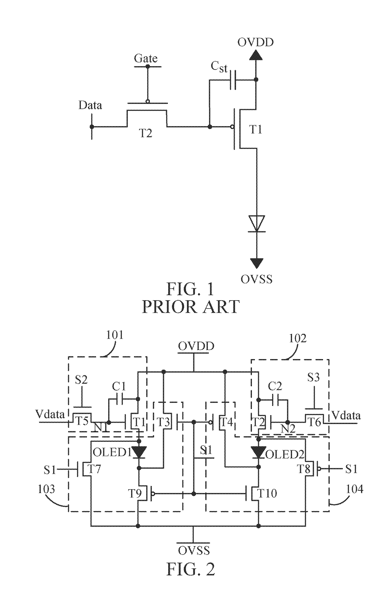
[0083]For better explaining the technical solution and the effect of the present disclosure, the present disclosure will be further described in detail with the accompanying drawings and the specific embodiments. The described embodiments are some but not all of the embodiments of the present disclosure. All other embodiments obtained by a person of ordinary skill in the art based on the embodiments of the present disclosure without creative efforts shall fall within the protection scope of the present disclosure.

[0084]Referring to FIG. 2, the present disclosure provides an OLED pixel circuit, including a first sub-pixel driving unit 101, a second sub-pixel driving unit 102, a first reverse biasing unit 103, and a second reverse biasing unit 104, wherein the first sub-pixel driving unit 101 includes a first thin-film transistor T1, a fifth thin-film transistor T5, a first capacitor C1, and a first light emitting diode OLED1; the second sub-pixel driving unit 102 includes a second th...


PUM


Abstract

The present disclosure provides an OLED pixel circuit and a method for retarding the aging of an OLED device. By providing a first sub-pixel driving unit, a second sub-pixel driving unit, a first reverse biasing unit, and a second reverse biasing unit and by simple control timing, a first light emitting diode and a second light emitting diode will not always be in a DC biased state, and the first light emitting diode and the second light emitting diode will emit light alternately in different frames.

Description

BACKGROUND OF THE INVENTIONField of the Invention[0001]The present disclosure relates to the technical field of display technology, and more particularly to an OLED pixel circuit and a method for retarding the aging of an OLED device.Description of the Related Art[0002]An Active Matrix Organic Light Emitting Diode (AMOLED) is able to emit light because it is driven by current generated by a driving Thin Film Transistor (TFT) in a saturated state, and a conventional AMOLED pixel circuit is generally a 2T1C driving circuit. Referring to FIG. 1, the 2T1C circuit includes two TFTs and one capacitor, wherein T1 is a driving transistor of the pixel circuit, and T2 is a switching transistor; the switching transistor T2 is turned on by a scanning line Gate, the storage capacitor Cst is charged by a data voltage Vdata, and the switching transistor T2 is turned off during the light emission; and, the voltage stored in the capacitor keeps the driving transistor T1 turned on, and the turn-on cu...

Claims


Application Information

Patent Timeline
IPC IPC(8): G09G3/3258
CPCG09G3/3258G09G2320/045G09G2300/0819G09G2310/08G09G3/3233G09G2300/0861G09G2310/0262
Inventor CHANG, BOBIAOCHEN, XIAOLONGWEN, YI-CHIEN
Owner SHENZHEN CHINA STAR OPTOELECTRONICS SEMICON DISPLAY TECH CO LTD
Why Eureka
Try Eureka