Hermetically sealed molecular spectroscopy cell with dual wafer bonding

a molecular spectroscopy and bonding technology, applied in the direction of layered products, electrical equipment, transmission, etc., can solve the problems of difficult formation of such structures, and achieve the effect of improving the radio frequency performance of antennas, transmission lines, and electromagnetic band gap structures

Active Publication Date: 2019-03-21
TEXAS INSTR INC
View PDF19 Cites 1 Cited by
  • Summary
  • Abstract
  • Description
  • Claims
  • Application Information

AI Technical Summary

Benefits of technology

[0003]In one embodiment, a method includes forming a plurality of layers of an oxide and a metal on a substrate. For example, the layers may include a metal layer sandwiched between silicon oxide layers. A non-conductive structure such as glass is then bonded to one of the oxide layers. An antenna can then be patterned on the non-conductive structure, and a cavity can be created in the substrate. Another metal layer is deposited on the surface of the cavity, and an iri

Problems solved by technology

Forming such structur

Method used


Image

  • Hermetically sealed molecular spectroscopy cell with dual wafer bonding
  • Hermetically sealed molecular spectroscopy cell with dual wafer bonding
  • Hermetically sealed molecular spectroscopy cell with dual wafer bonding

Examples


Embodiment Construction

[0010]In this description, the term “couple” or “couples” means either an indirect or direct wired or wireless connection. Thus, if a first device couples to a second device, that connection may be through a direct connection or through an indirect connection via other devices and connections. Also, in this description, the recitation “based on” means “based at least in part on.” Therefore, if X is based on Y, then X may be a function of Y and any number of other factors.

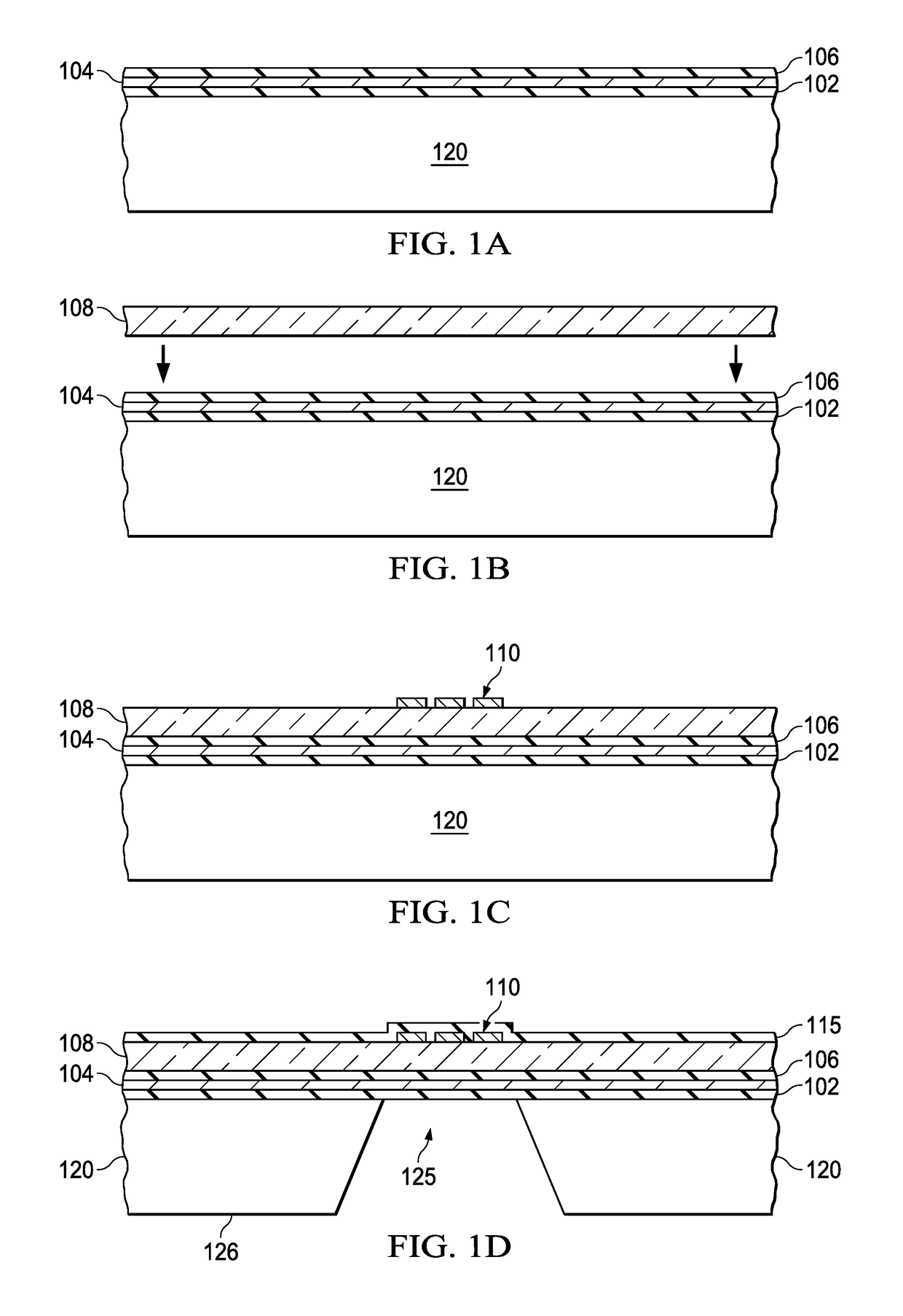
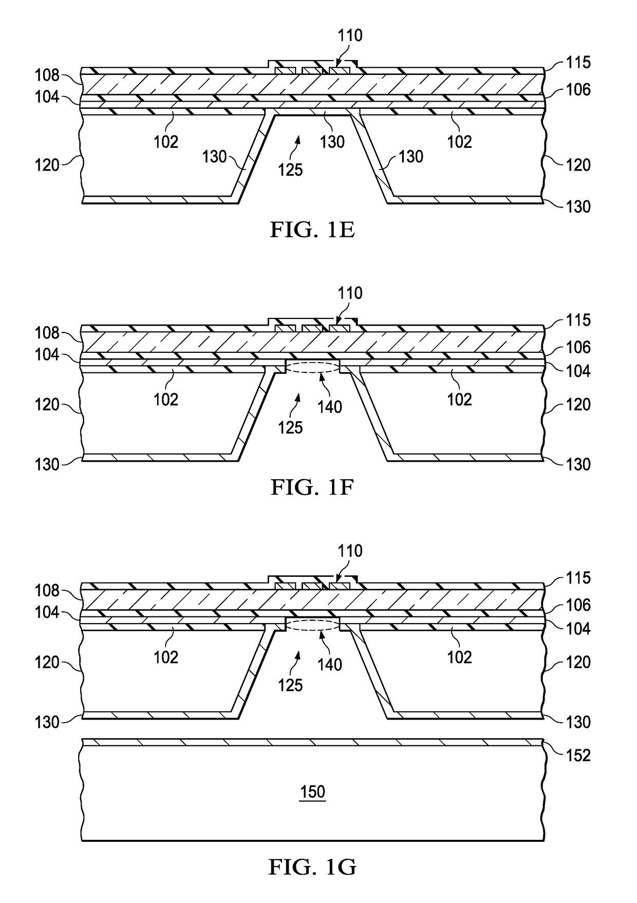
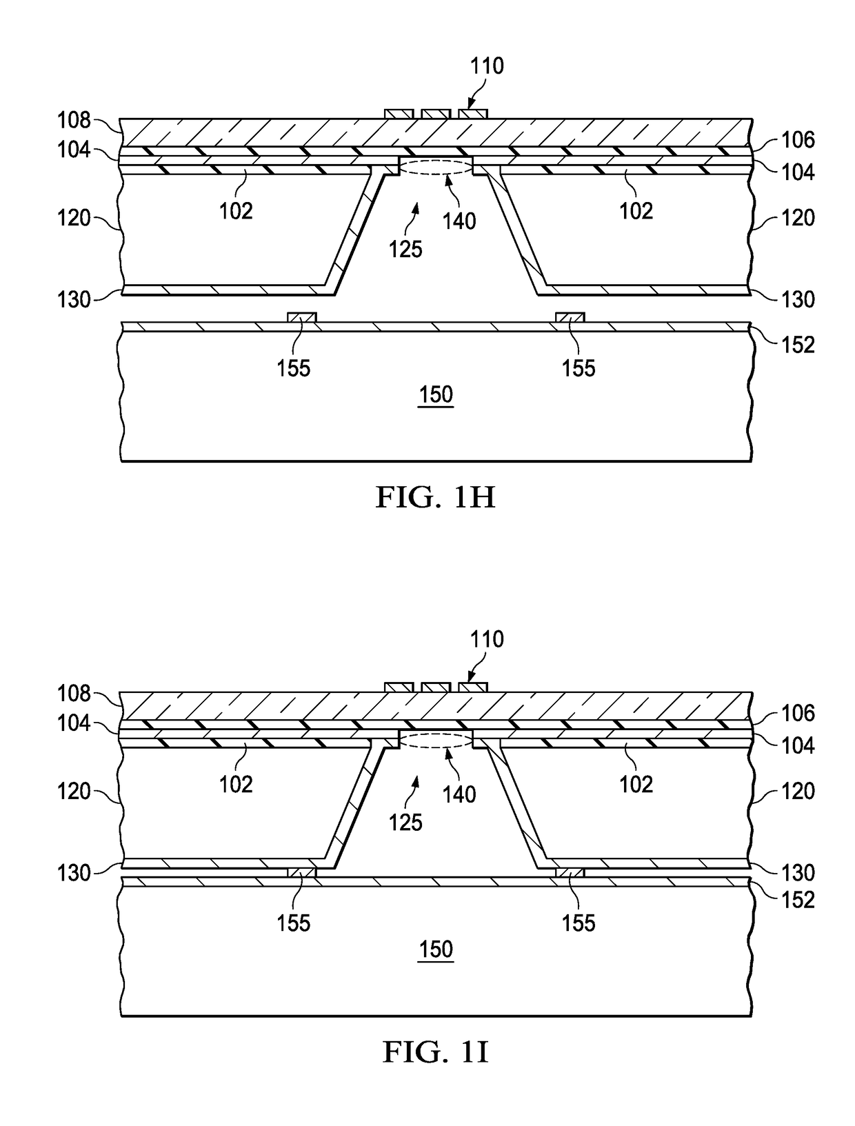
[0011]The disclosed embodiments of the present disclosure include techniques to fabricate a hermetically sealed cavity in a substrate. A structure containing a substrate with the cavity may be used in numerous applications. One illustrative use is as a millimeter wave chip scale atomic clock. The cavity may contain a plurality of dipolar molecules (e.g., water molecules) at a relatively low pressure. For some embodiments, the pressure may be approximately 0.1 mbarr for water molecules. If argon molecules were used, ...


PUM


Abstract

A method includes forming a plurality of layers of an oxide and a metal on a substrate. For example, the layers may include a metal layer sandwiched between silicon oxide layers. A non-conductive structure such as glass is then bonded to one of the oxide layers. An antenna can then be patterned on the non-conductive structure, and a cavity can be created in the substrate. Another metal layer is deposited on the surface of the cavity, and an iris is patterned in the metal layer to expose the one of the oxide layers. Another metal layer is formed on a second substrate and the two substrates are bonded together to thereby seal the cavity.

Description

CROSS-REFERENCE TO RELATED APPLICATIONS[0001]This application is a continuation of U.S. patent application Ser. No. 15 / 698,346 filed Sep. 7, 2017, which is fully incorporated herein by reference.BACKGROUND[0002]Various applications may include a sealed chamber formed in a semiconductor structure. In one particular application, a chip-scale atomic clock may include a selected vapor at a low pressure in a sealed chamber. Forming such structures can be a challenge.SUMMARY[0003]In one embodiment, a method includes forming a plurality of layers of an oxide and a metal on a substrate. For example, the layers may include a metal layer sandwiched between silicon oxide layers. A non-conductive structure such as glass is then bonded to one of the oxide layers. An antenna can then be patterned on the non-conductive structure, and a cavity can be created in the substrate. Another metal layer is deposited on the surface of the cavity, and an iris is patterned in the metal layer to expose the one...

Claims


Application Information

Patent Timeline
IPC IPC(8): B32B7/04H04B1/38
CPCB32B7/04H04B1/38G04F5/14H04B1/3827H04B2001/3894
Inventor FRUEHLING, ADAM JOSEPHHERBSOMMER, JUAN ALEJANDROCOOK, BENJAMIN STASSENJACOBS, SIMON JOSHUA
Owner TEXAS INSTR INC
Why Eureka
Try Eureka