Optical film and display body
a technology of optical film and display body, which is applied in the direction of instruments, printing, hologram form/shape, etc., can solve the problems that the technology suited to simultaneously tackle these challenges has not been implemented, and the reconstruction image cannot be obtained only under the conditions, so as to reduce the computing time and maximize the contrast of the reconstructed image
- Summary
- Abstract
- Description
- Claims
- Application Information
AI Technical Summary
Benefits of technology
Problems solved by technology
Method used
Image
Examples
first embodiment
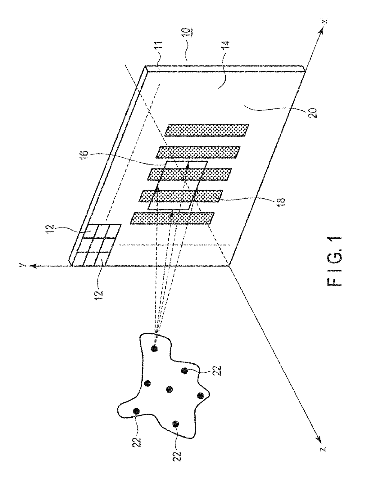
[0096]FIG. 1 is a schematic diagram illustrating an optical film according to a first embodiment of the present invention.
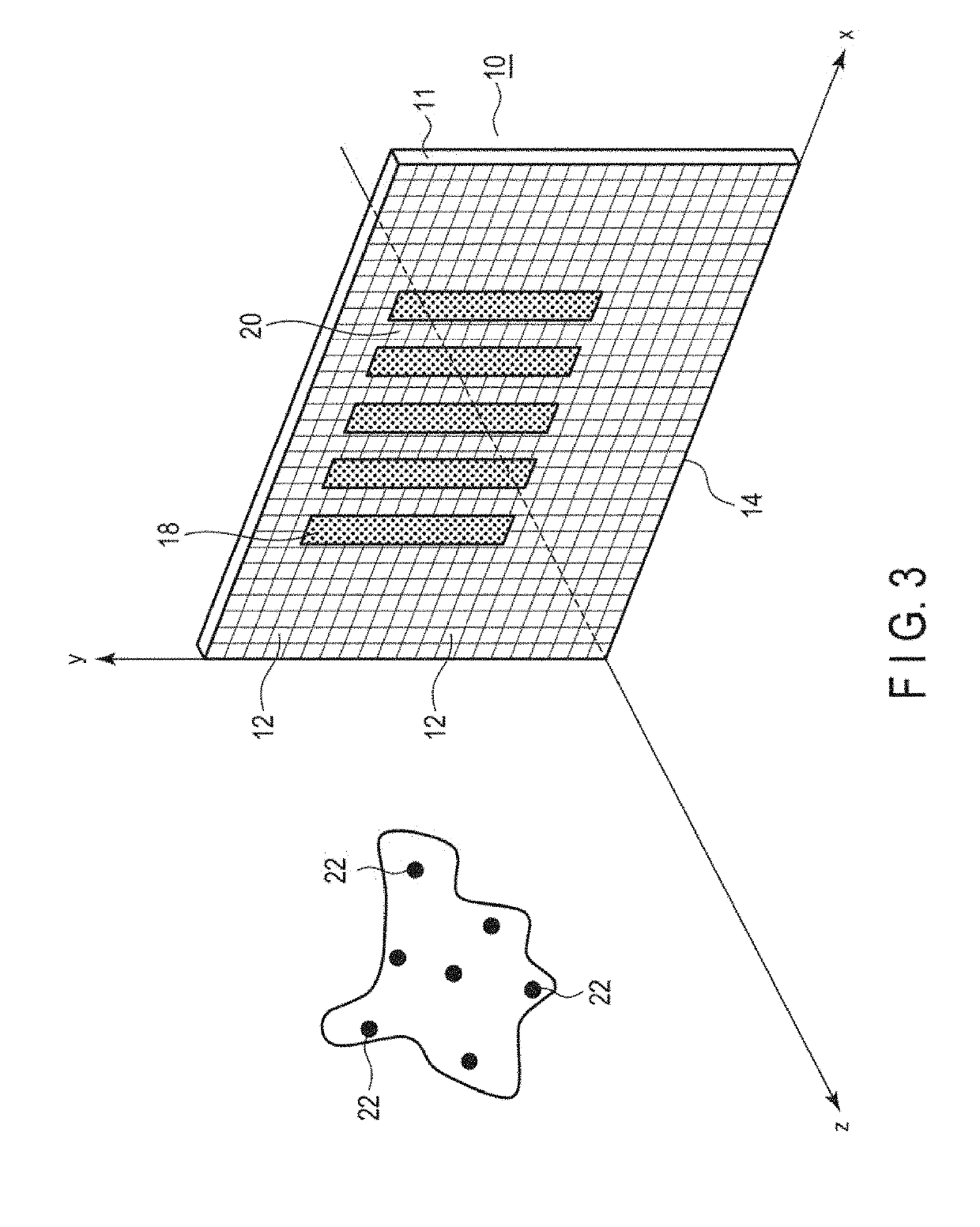
[0097]An optical film 10 according to the embodiment includes a recording surface 14. The recording surface 14 is provided on a surface of a substrate 11.
[0098]The recording surface 14 includes a phase angle recording area 18 and a phase angle non-recording area 20. On the recording surface 14, an area other than the phase angle recording area 18 is the phase angle non-recording area 20. In one example, the phase angle non-recording area 20 is a mirror surface.
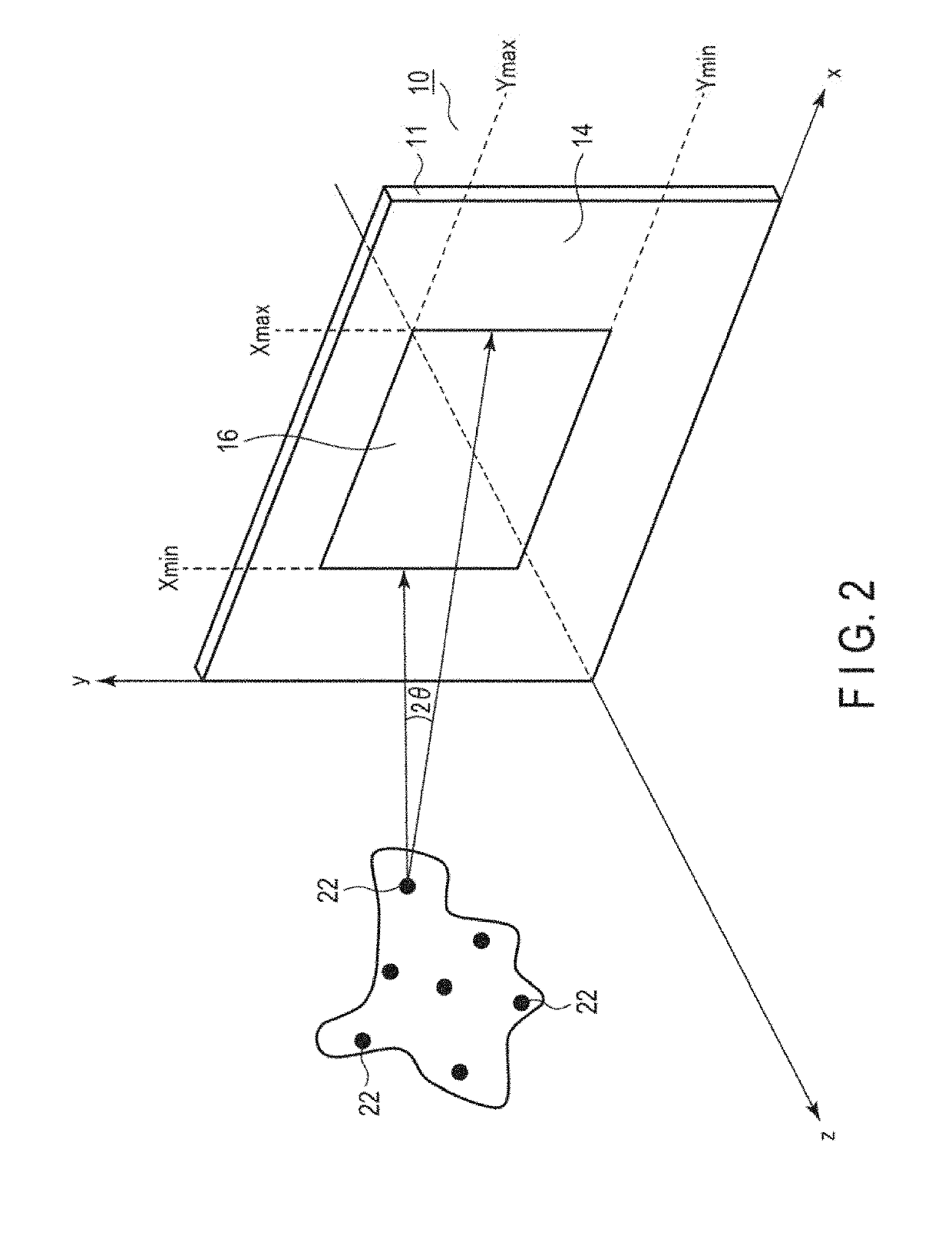
[0099]FIG. 2 is a diagram illustrating a viewing angle θ when a viewing angle direction is the X direction.
[0100]On the recording surface 14, a computation element section 16 is defined in accordance with the viewing angle θ from each reconstruction point 22 where a reconstructed image is reconstructed. Since the computation element section 16 is defined independently of the phase angle recording area 18 an...
second embodiment
[0144]In the first embodiment, the case of recording the numerical information of the corresponding phase angle φ in the unit block 12 in the overlapping area 19 is described. In the optical film 10 according to the present embodiment, instead of recording the numerical information of the phase angle φ in the unit block 12 in the overlapping area 19, the computing device converts the phase angle φ to a height of the unevenness of the corresponding unit block 12 and forms the unevenness having the height corresponding to the phase angle φ in the unit block 12 of the overlapping area 19, thereby recording the phase angle φ in the unit block 12 of the overlapping area 19.
[0145]FIG. 12 is a cross-sectional diagram showing an example of the optical film 10 including the unit block 12 having unevenness corresponding to the phase angle cp.
[0146]When converting the phase angle φ to a height of the unevenness, the computing device computes a phase angle φ in the range of 0 to 2 π, and furthe...
third embodiment
[0192]In the first embodiment, the case of recording the numerical information of the corresponding phase angle φ in the unit block 12 in the overlapping area 19 is described. In the optical film 10 according to the present embodiment, instead of recording the numerical information of the phase angle φ, the computing device converts the change in the phase angle φ into the amount of change of the refractive index of the recording surface 14. Also, the computing device converts it into a void that realizes the amount of change of the refractive index. The phase angle φ is recorded in the unit block 12 in the overlapping area 19 by embedding the void 23 in the substrate 11 corresponding to the location of the unit block 12 in the overlapping area, for example, as shown in FIG. 25.
[0193]As described above, according to the optical film 10 of the present embodiment, the change in the phase angle φ is converted into the amount of change of the refractive index of the recording surface 14...
PUM
 Abstract
Description
Claims
Application Information


