Display device and method for manufacturing display device

a display device and display device technology, applied in the direction of solid-state devices, sustainable manufacturing/processing, final product manufacturing, etc., can solve the problems of wire cracking and wire cracking, and achieve the effect of reducing the frame siz

Active Publication Date: 2019-04-04
JAPAN DISPLAY INC
View PDF5 Cites 6 Cited by
  • Summary
  • Abstract
  • Description
  • Claims
  • Application Information

AI Technical Summary

Benefits of technology

[0005]An object of the present invention is to reduce a frame size without damaging wiring.

Problems solved by technology

This may cause damage, such as a crack, on the wires due to bending stress generated at that time.

Method used


Image

  • Display device and method for manufacturing display device
  • Display device and method for manufacturing display device
  • Display device and method for manufacturing display device

Examples


first embodiment

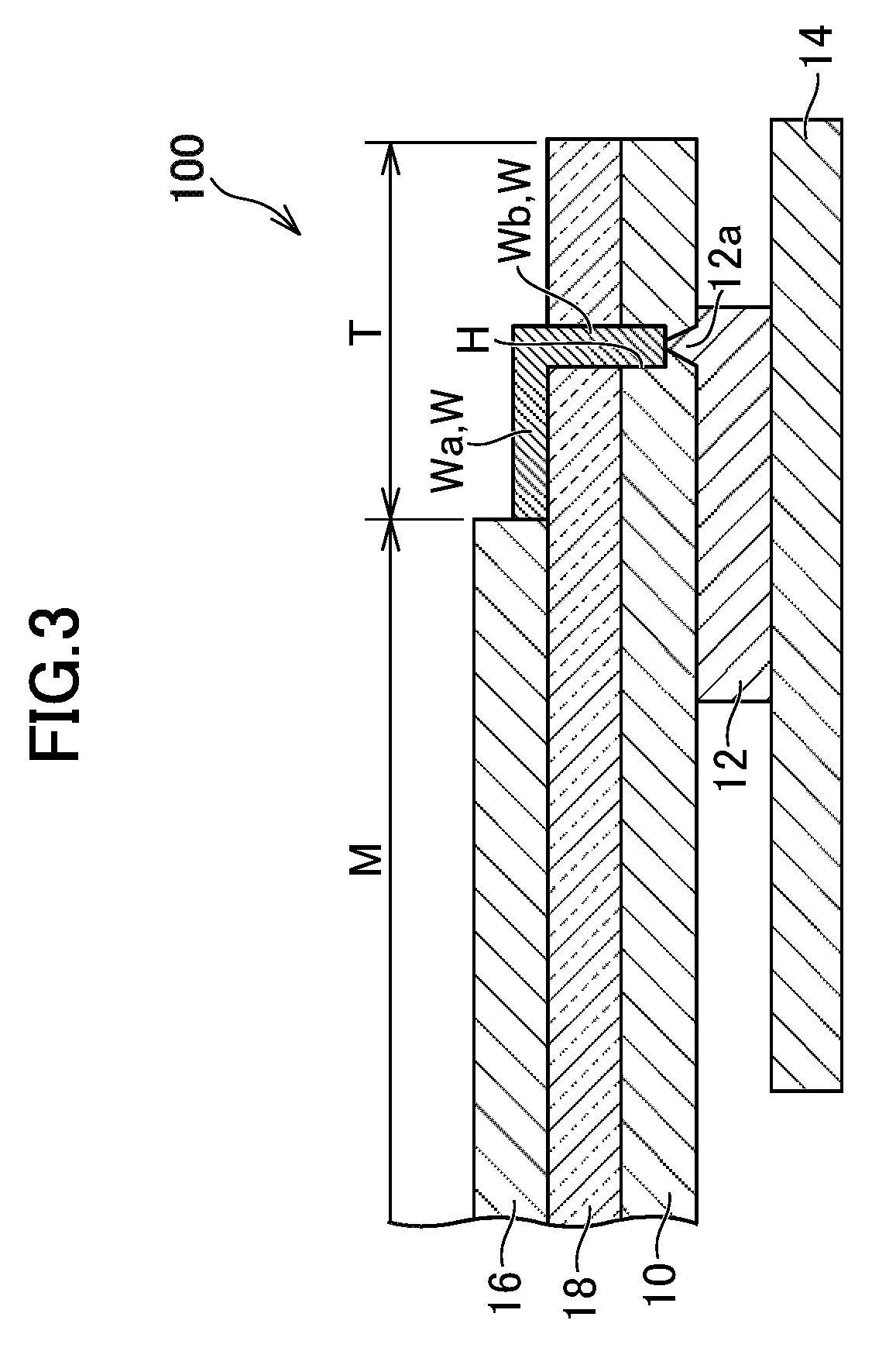
[0030]Next, referring to FIGS. 1 to 3, the connection between the circuit layer 16 and electronic components in the first embodiment will be described. FIG. 3 is a cross sectional view of the display device taken along the line III-III in FIG. 1.

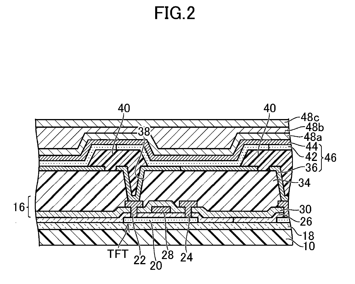
[0031]As described by reference to FIG. 2, the inorganic film 18 is disposed on the resin substrate 10, and the circuit layer 16 is disposed on the inorganic film 18. In this regard, as described by reference to FIG. 2, the layers such as the organic electroluminescence layer 42 are disposed on the circuit layer 16, although not shown in FIG. 3.

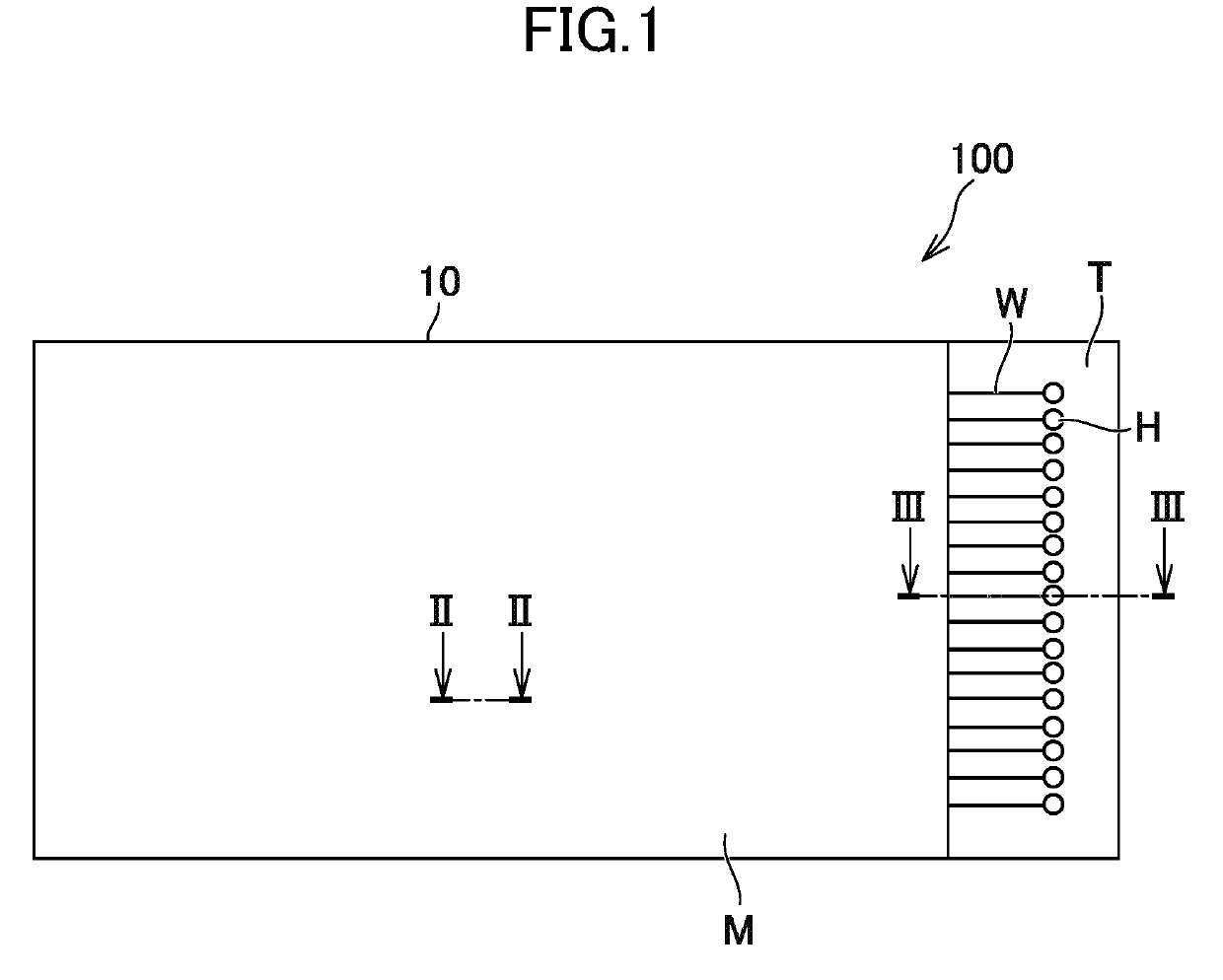
[0032]An IC driver 12 is disposed on the side of the resin substrate 10 opposite to the side on which the circuit layer 16 is disposed. The IC driver 12 is an electronic component mounted on the resin substrate 10 as a chip on glass (COG), and sends a driving signal to the display area M through wires W described later. As shown in FIGS. 1 and 3, the wires W are formed on the resin substrate 10 so as ...

second embodiment

[0046]In the display device 200 the wire W1 and the wire W2 are not bent along the bending of the resin substrate 10. As such, these wires are not damaged due to bending stress, for example. The bent portion of the inorganic film 18 shown in FIG. 6 may be removed.

[0047]Next, with reference to FIGS. 6 to 10, a manufacturing process of the display device according to the second embodiment will be described. FIGS. 7 to 10 are diagrams for explaining the manufacturing process of the display device according to the second embodiment.

[0048]First, a glass substrate 50 is prepared. Then, a resin substrate 10 having flexibility (flexible substrate) is disposed on the glass substrate 50. The resin substrate 10 is thus disposed on the glass substrate 50 having high stiffness, which facilitates the subsequent laminating process. Further, an inorganic film 18 is disposed on the resin substrate 10. Subsequently, holes h1 and h2 are formed by etching in an area, which corresponds to the terminal ...


PUM


Abstract

A display device includes a resin substrate including a through hole in a terminal area around a display area in which an image is displayed, a circuit layer including a thin film transistor and disposed in the display area on the resin substrate, a wire extending from the circuit layer and formed inside of the through hole, and an IC driver disposed on a side of the resin substrate opposite to a side on which the circuit layer is disposed. The IC driver includes a terminal that protrudes into the through hole and is in contact with the wire formed inside of the through hole such that the IC driver and the circuit layer are electrically connected to each other.

Description

CROSS-REFERENCE TO RELATED APPLICATION[0001]The present application claims priority from Japanese application JP2017-190353 filed on Sep. 29, 2017, the content of which is hereby incorporated by reference into this application.BACKGROUND OF THE INVENTION1. Field of the Invention[0002]The present invention relates to a display device and a method for manufacturing the display device.2. Description of the Related Art[0003]Display devices having a flexible substrate have been known. Such display devices reduce a frame size by bending areas around a display area and disposing a terminal area, on which electronic components are mounted, on the back side of the display area (e.g., JP2011-209405A).[0004]As disclosed in JP2011-209405A, when bending the flexible substrate, wires on the flexible substrate also need to be bent. This may cause damage, such as a crack, on the wires due to bending stress generated at that time.SUMMARY OF THE INVENTION[0005]An object of the present invention is to...

Claims


Application Information

Patent Timeline
Patent Type & Authority Applications(United States)
IPC IPC(8): H01L27/12H01L51/50H01L51/56H01L27/32H01L51/00
CPCH01L27/124H01L51/5012H01L51/56H01L27/3244H01L51/0097H01L27/1218Y02E10/549Y02P70/50H10K59/131H10K77/111H10K71/80H10K59/1201H10K50/11H10K59/12H10K71/00
Inventor NAKAIE, HIROKI
Owner JAPAN DISPLAY INC
Why Eureka
Try Eureka