

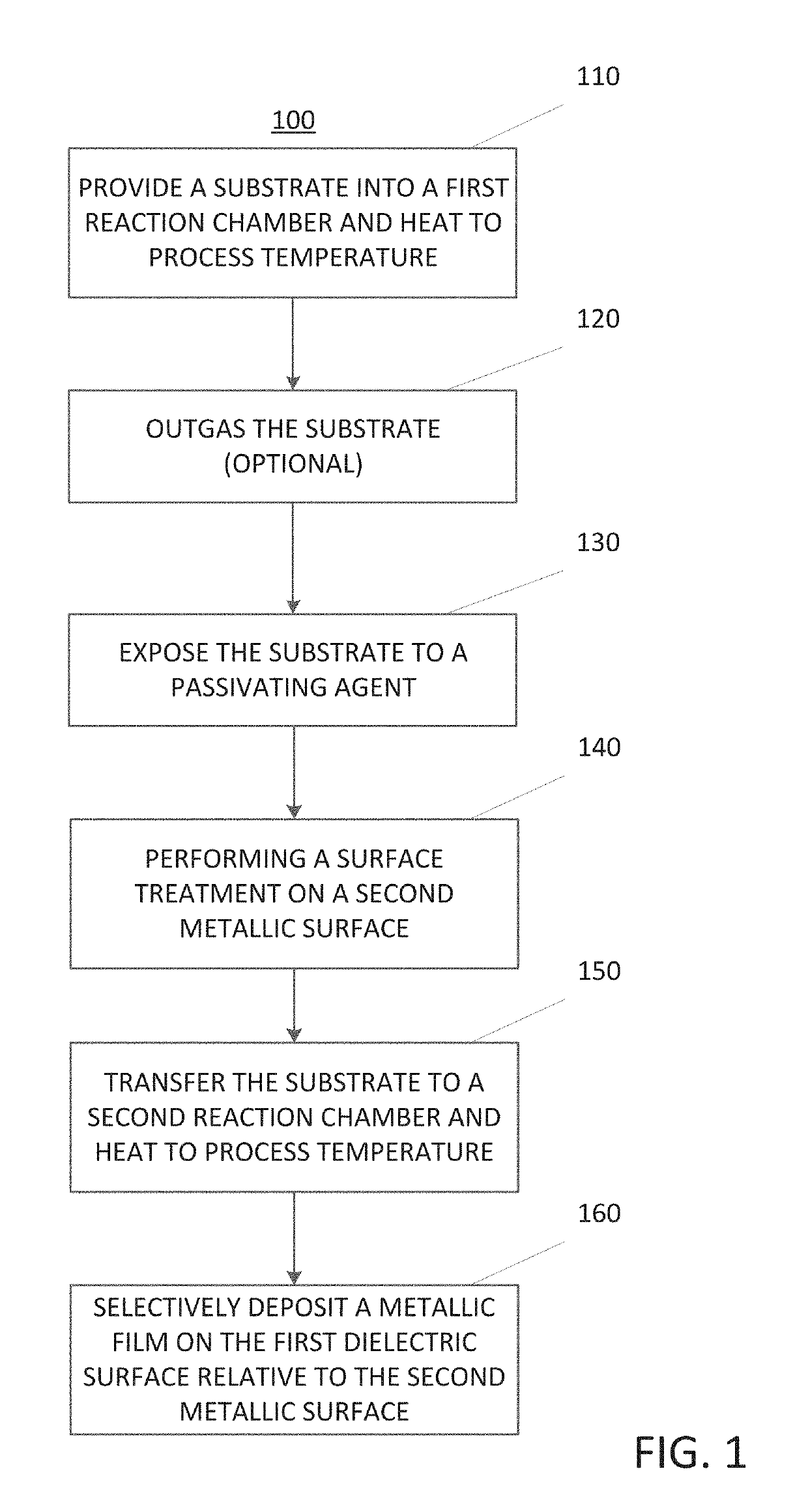
Method for selectively depositing a metallic film on a substrate
a technology of metallic film and substrate, which is applied in the direction of coating, chemical vapor deposition coating, semiconductor devices, etc., can solve the problems of time-consuming and expensive lithography and etch process, and inability to meet the requirements of many applications
- Summary
- Abstract
- Description
- Claims
- Application Information
AI Technical Summary
Benefits of technology
Problems solved by technology
Method used
Image

Examples
Embodiment Construction
[0012]Although certain embodiments and examples are disclosed below, it will be understood by those in the art that the invention extends beyond the specifically disclosed embodiments and / or uses of the invention and obvious modifications and equivalents thereof. Thus, it is intended that the scope of the invention disclosed should not be limited by the particular disclosed embodiments described below.
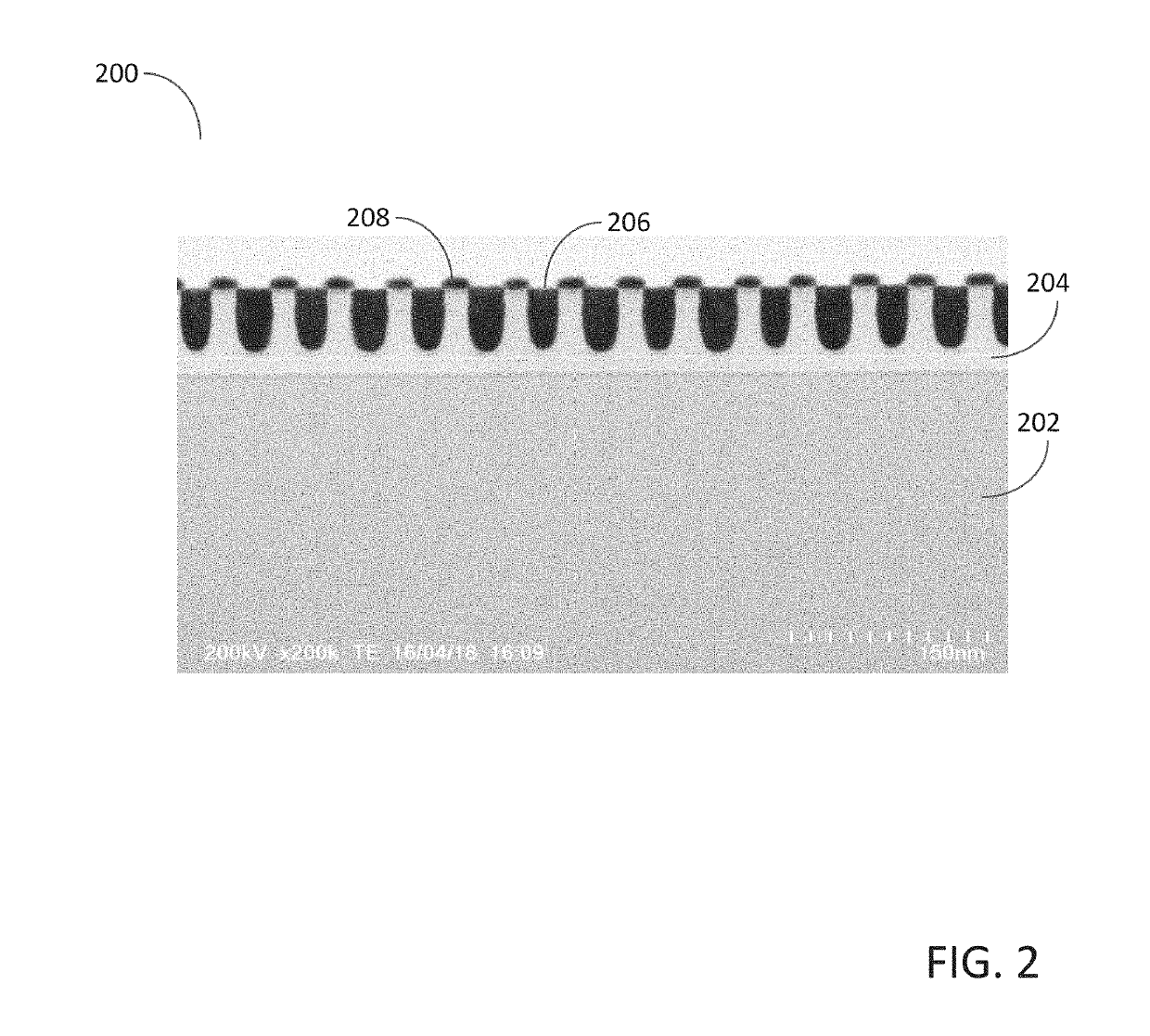
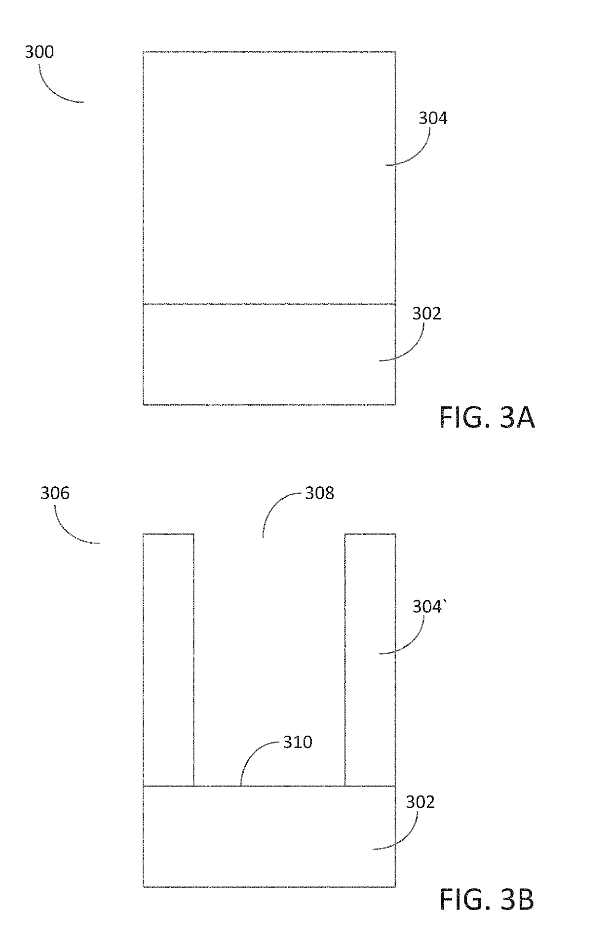
[0013]The illustrations presented herein are not meant to be actual views of any particular material, structure, or device, but are merely idealized representations that are used to describe embodiments of the disclosure.
[0014]As used herein, the term “substrate” may refer to any underlying material or materials that may be used, or upon which, a device, a circuit or a film may be formed.
[0015]As used herein, the term “passivating agent” may refer to any chemical species which when applied to a surface of a material, alters at least the surface of that material in a manner which will r...
PUM
| Property | Measurement | Unit |
|---|---|---|
| temperature | aaaaa | aaaaa |
| time period | aaaaa | aaaaa |
| temperature | aaaaa | aaaaa |
Abstract
Description
Claims
Application Information