Device and method for charge removal from dielectric surfaces

a dielectric surface and charge technology, applied in the direction of electrostatic charges, emergency protective circuit arrangements, coatings, etc., can solve the problems of high handling difficulty, health risk to people, and disturbance in the system used, so as to improve the efficiency of electric charge removal and optimize the homogeneity of plasma

Inactive Publication Date: 2005-08-23
ROBERT BOSCH GMBH
View PDF9 Cites 57 Cited by
  • Summary
  • Abstract
  • Description
  • Claims
  • Application Information

AI Technical Summary

Benefits of technology

[0006]The device and method according to the present invention have the advantage over the related art that they yield an optimized charge removal from dielectric surfaces, in particular surfaces of plastic films, paper webs, or plastic fibers with regard to the magnitude of the electric residual voltage, i.e., the electric charge remaining at the surface and thus also yield a definite improvement in manufacturing stability and simplified handling of such dielectric materials. To this extent, the device and method according to the present invention are suitable for use in the packaging industry in particular.
[0009]In addition, the method according to the present invention has the advantage that typical treatment times of 0.1 s to 10 s, in particular 0.5 s to 2 s, which are definitely shortened in comparison with the related art, are sufficient to guarantee adequate removal of electric charges from the dielectric surface to be treated. In particular, continuous treatment of continuous films or webs of a dielectric material using the device according to the present invention is also possible.
[0010]Moreover, due to the removal of electric charges from dielectric surfaces performed according to the present invention, activation of these surfaces in particular with regard to the surface energy and cleanliness is also achieved at the same time, which is manifested in improved imprintability and increased hydrophilic characteristics, for example.
[0011]Finally, the device according to the present invention has the advantage of a simple and modular design, so it is integratable into existing manufacturing systems without requiring complex equipment. Furthermore, the method according to the present invention may also be used in air at atmospheric pressure.
[0013]With regard to an optimized homogeneity of the plasma thus produced and an improved efficiency of the removal of electric charges from the dielectric surface thus achieved, it is also advantageous if this work is performed at a low partial vacuum of 100 mbar to 900 mbar in particular. In addition it is advantageous if instead of air, nitrogen or, especially advantageously, argon or helium is used as the gas to generate a plasma which is as homogeneous and stable as possible.

Problems solved by technology

The electric charge buildup on surfaces may also result in a disturbance in the systems used as well as constitute a health risk to people working on these systems in the production and / or processing of those surfaces.
Furthermore, handling is much more difficult due to the electric charge on the surface and the resulting electrostatic forces, in particular in the case of plastic films, paper webs, or plastic fibers, such as those widely used in the packaging industry.

Method used


Image

  • Device and method for charge removal from dielectric surfaces
  • Device and method for charge removal from dielectric surfaces
  • Device and method for charge removal from dielectric surfaces

Examples


Embodiment Construction

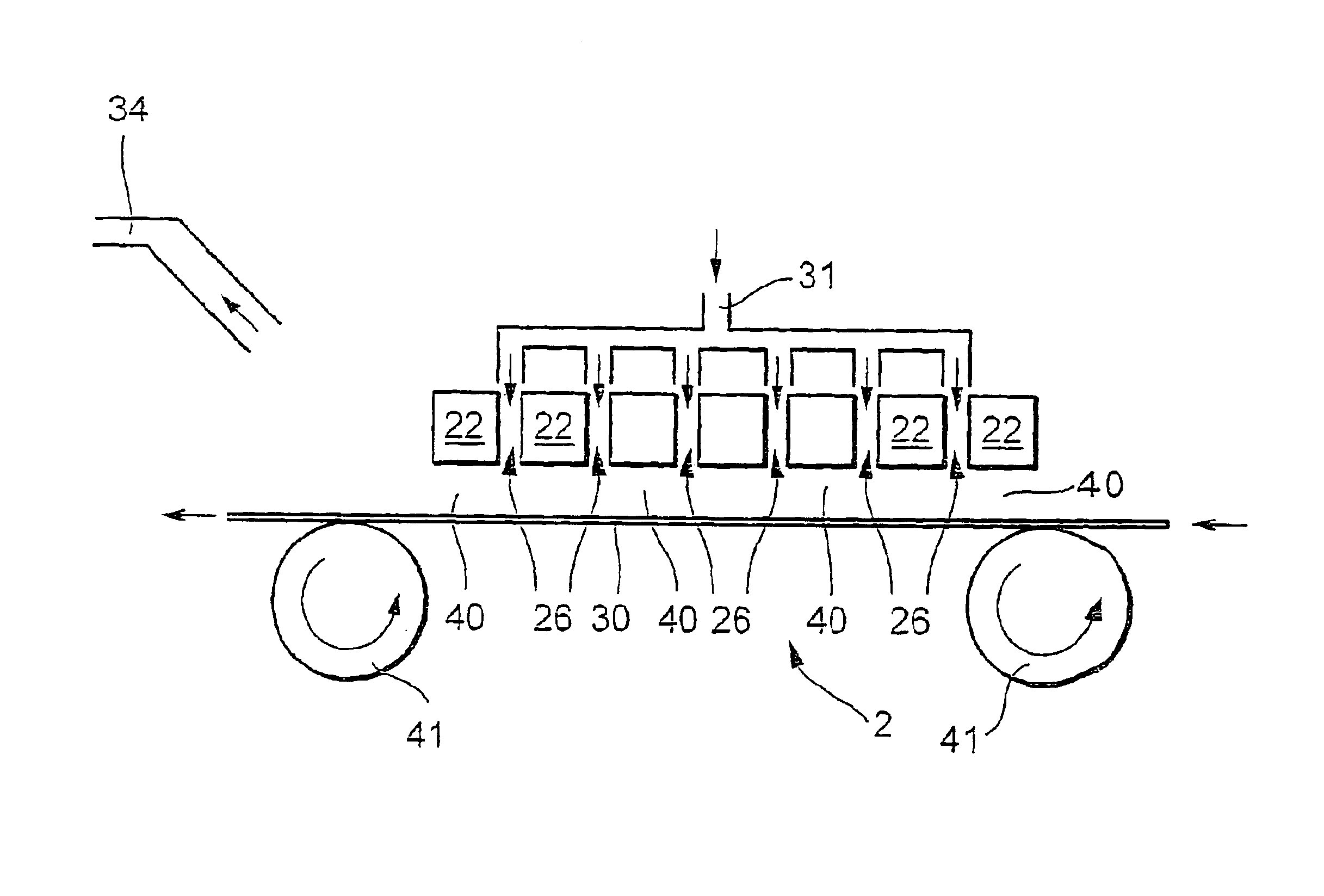
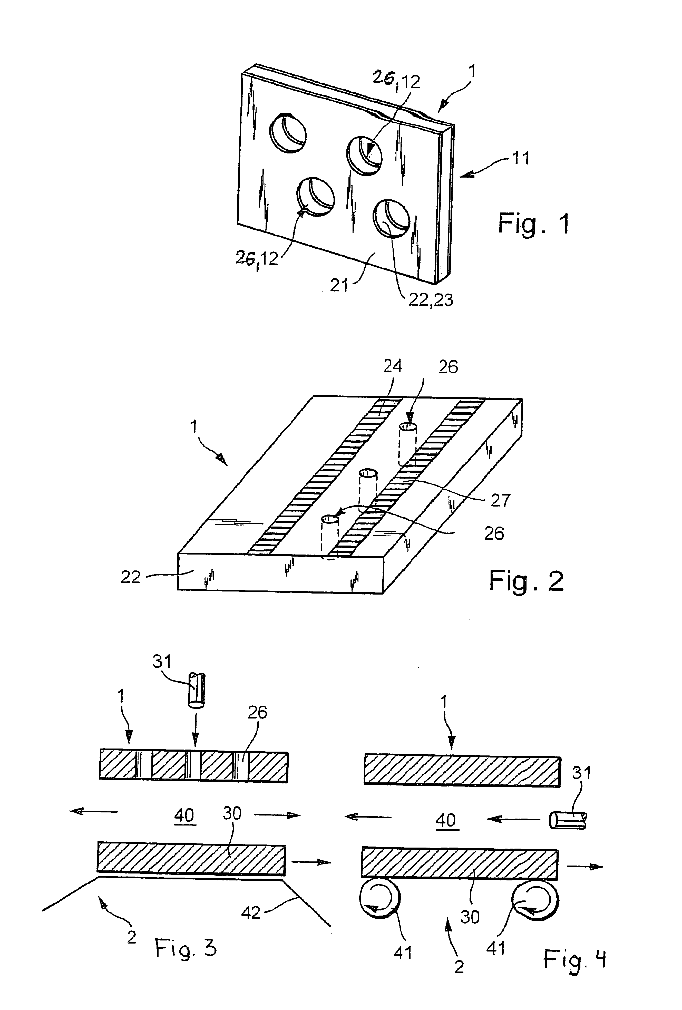
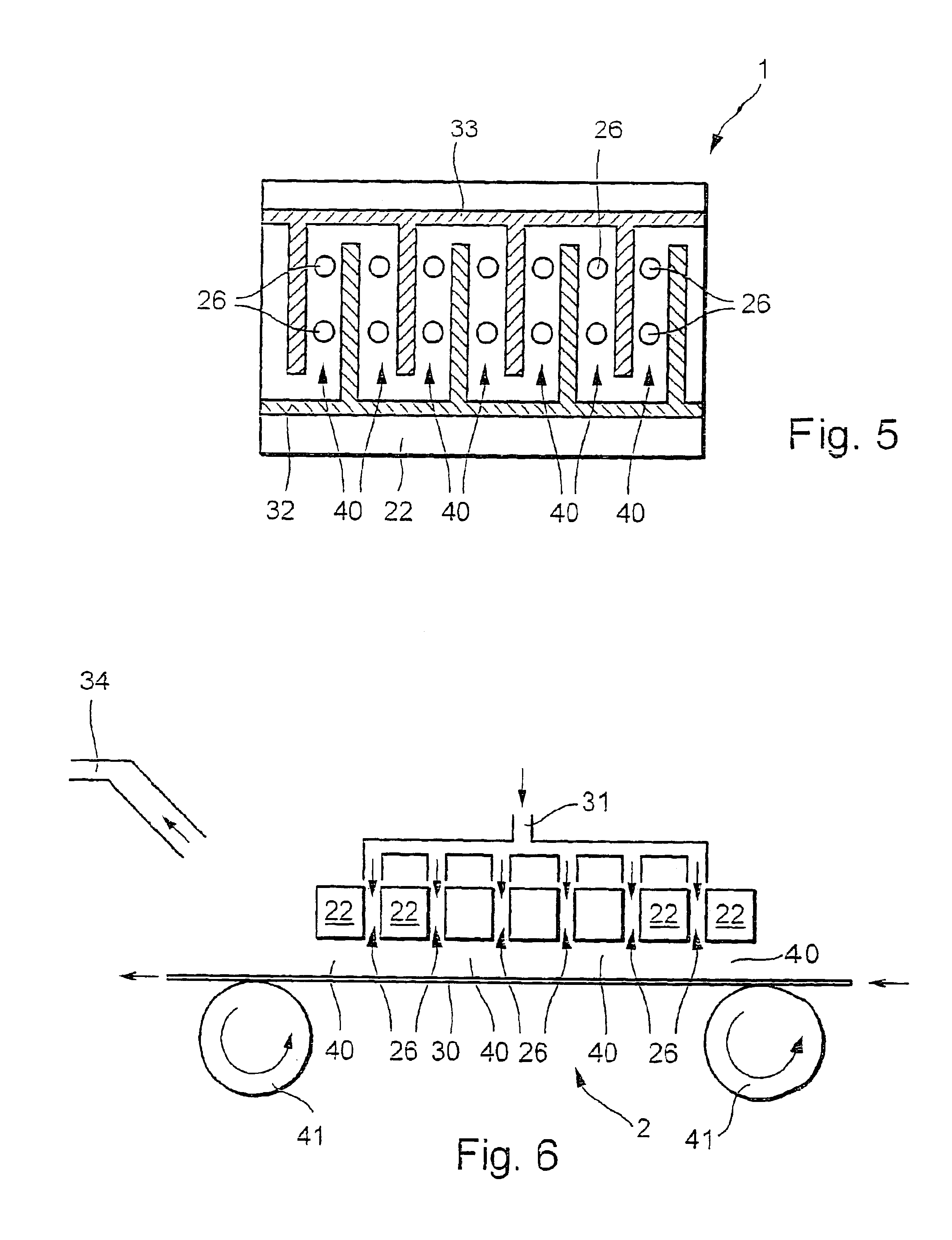
[0022]FIG. 1 shows a plasma device 1 having a dielectric plate 22 made of a low-loss puncture proof dielectric such as silicon dioxide or an aluminum oxide, for example. Dielectric plate 22 is also provided with a planar first electrode 11 on one of its surfaces and a planar second electrode 21 on the diametrically opposite surface. Electrodes 11, 21 are made of a metal such as copper, high-grade steel, gold, or silver, for example, and are applied in the form of a coating 10 μm to 200 μm thick on the surface of dielectric plate 22, which is typically approx. 0.05 mm to 2 mm thick.

[0023]FIG. 1 also shows that electrodes 11, 21 and dielectric plate 22 are provided with a plurality of common through-bores 26. These through-bores 26 are preferably laid out in a regular pattern and have a typical diameter of approx. 40 μm to 1 mm. Thus on the whole dielectric plate 22 is provided with microstructured planar electrodes 11, 21.

[0024]To generate a plasma, electrodes 11, 21 in FIG. 1 are co...


PUM

PropertyMeasurementUnit
diameteraaaaaaaaaa
electric voltageaaaaaaaaaa

Abstract

A device and a method for at least partial removal of electric charges from dielectric surfaces, in particular surfaces of plastic films, paper webs or plastic fibers are described. First, a plasma is generated through microstructure discharges with a plasma device in at least one plasma region. In addition, the dielectric surface is introduced into the plasma region with a feed mechanism and is temporarily exposed to electrically charged particles generated by the plasma there.

Description

FIELD OF THE INVENTION[0001]The present invention relates to a device and a method for at least partial removal of electric charges from dielectric surfaces.BACKGROUND INFORMATION[0002]Nonconducting substances such as surfaces of plastic films, paper webs, or plastic fibers may develop an electric charge at the surface by coming in contact with other substances or due to rapid separation from one another, and the resulting electric voltage on such surfaces may reach a few megavolts. “Natural” unassisted charge removal may take a few hours to days, depending on atmospheric humidity, the type of material and the magnitude of the electric charge.[0003]The electric charge buildup on surfaces may also result in a disturbance in the systems used as well as constitute a health risk to people working on these systems in the production and / or processing of those surfaces. Furthermore, handling is much more difficult due to the electric charge on the surface and the resulting electrostatic fo...

Claims


Application Information

Patent Timeline
Patent Type & Authority Patents(United States)
IPC IPC(8): H01J37/02H05F3/04H05F3/00C23C16/50C08J7/00C23C16/511H01J37/32
CPCH01J37/026H01J37/32752H05F3/04H01J2237/0044H01J2237/336
Inventor GROSSE, STEFANHENKE, SASCHA
Owner ROBERT BOSCH GMBH
Why Eureka
Try Eureka