Pad bonding employing a self-aligned plated liner for adhesion enhancement

a self-aligned, plated technology, applied in the direction of electrical equipment, semiconductor devices, semiconductor/solid-state device details, etc., can solve the problems of limiting the effectiveness of fusing dielectric materials or grain growth of metal across the original, the temperature of the bonded substrate cannot be raised above a certain limit, and the effect of improving mechanical adhesion

Active Publication Date: 2011-04-14
TAIWAN SEMICON MFG CO LTD
View PDF25 Cites 60 Cited by
  • Summary
  • Abstract
  • Description
  • Claims
  • Application Information

AI Technical Summary

Benefits of technology

[0008]According to yet another aspect of the present invention, a method of forming a bonded structure is provided. The method includes bringing a first substrate and a second substrate into contact with each other, wherein a first surface of a first metal pad embedded in the first substrate contacts a second surface of a se...

Problems solved by technology

The effectiveness of currently available bonding methods is limited by the bonding strength, i.e., the mechanical adhesion strength, between the two substrates that are bonded together.
Because substrates including semiconductor devices are bonded after semiconductor devices are fully formed within each substrate, the temperature of bonded substrate...

Method used


Image

  • Pad bonding employing a self-aligned plated liner for adhesion enhancement
  • Pad bonding employing a self-aligned plated liner for adhesion enhancement
  • Pad bonding employing a self-aligned plated liner for adhesion enhancement

Examples


first embodiment

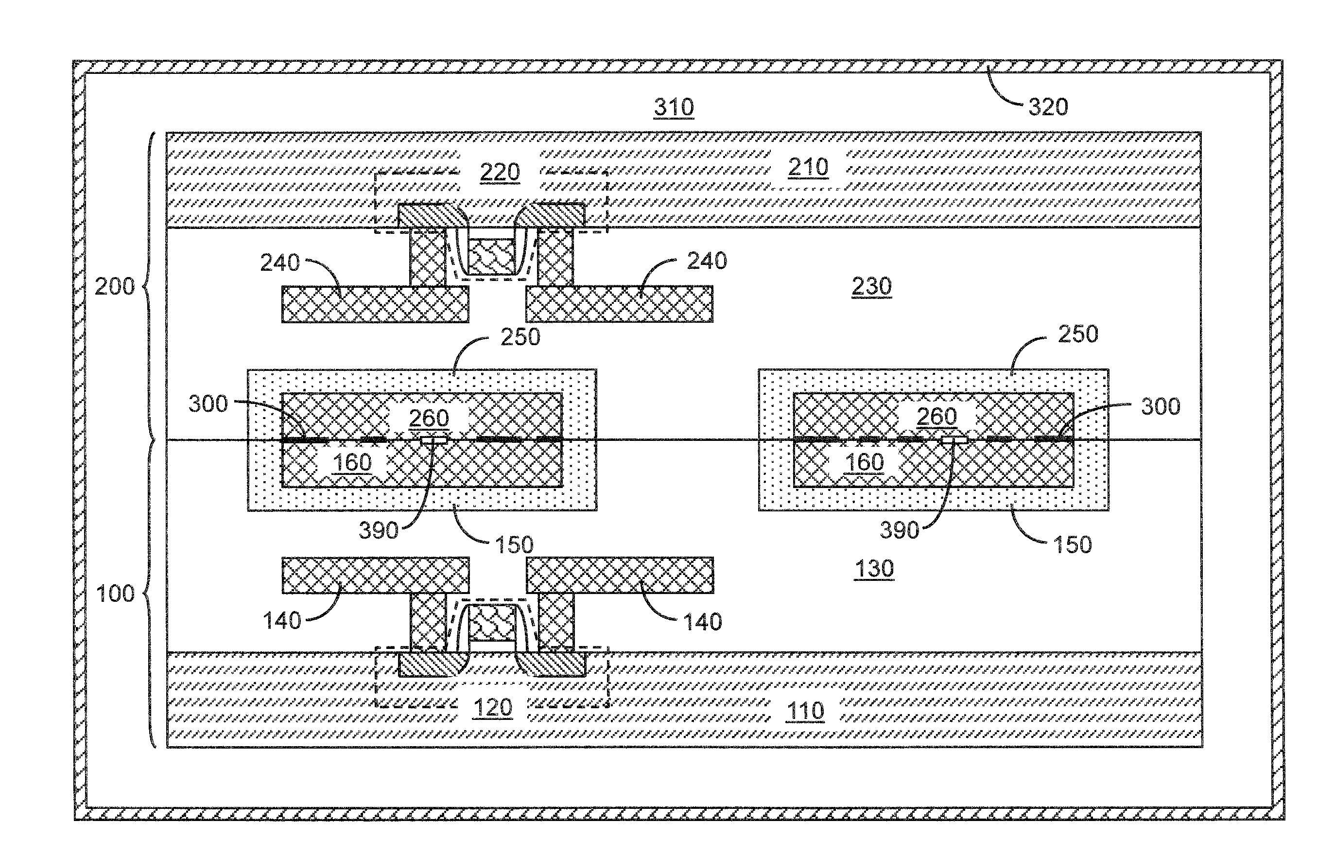
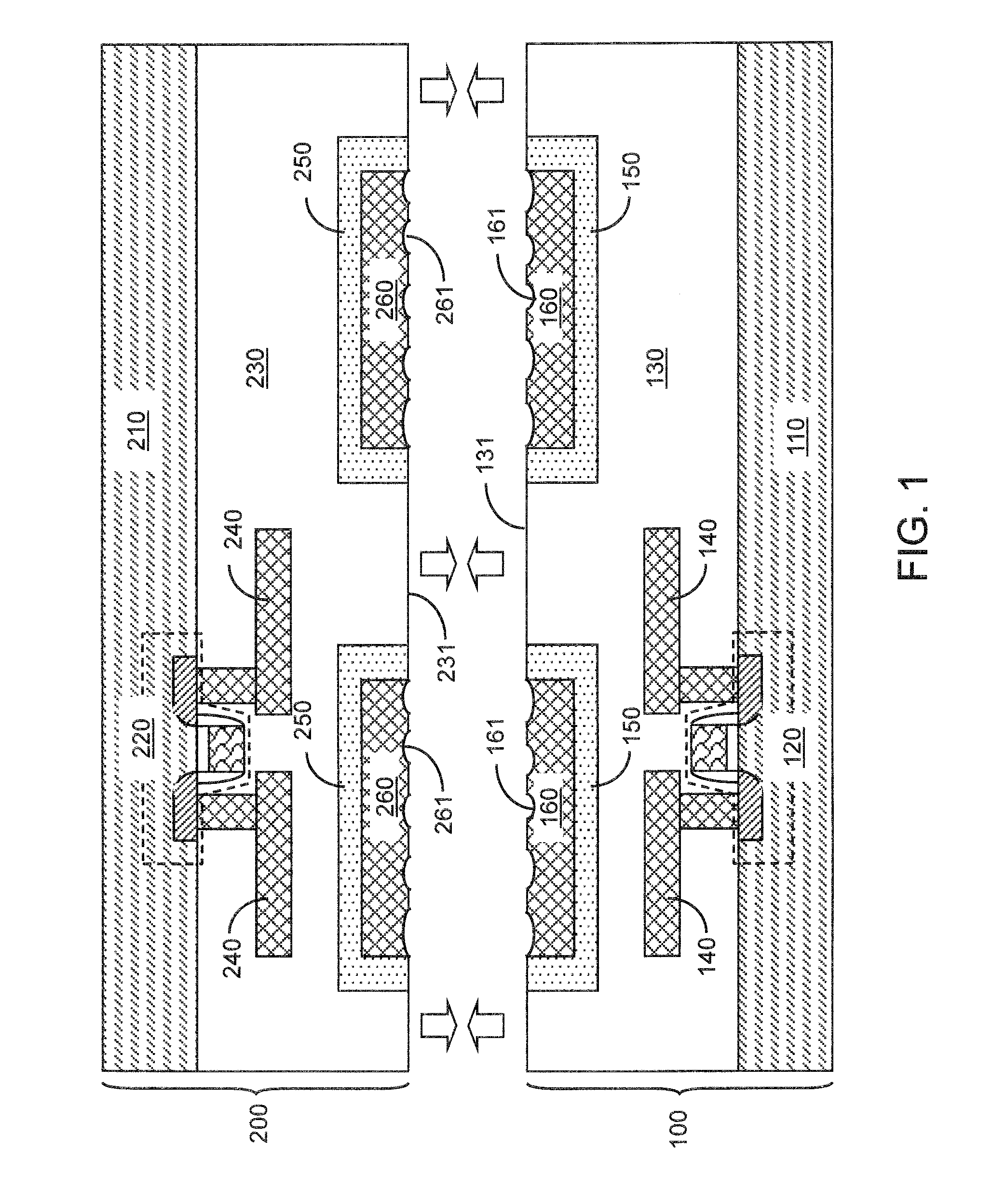
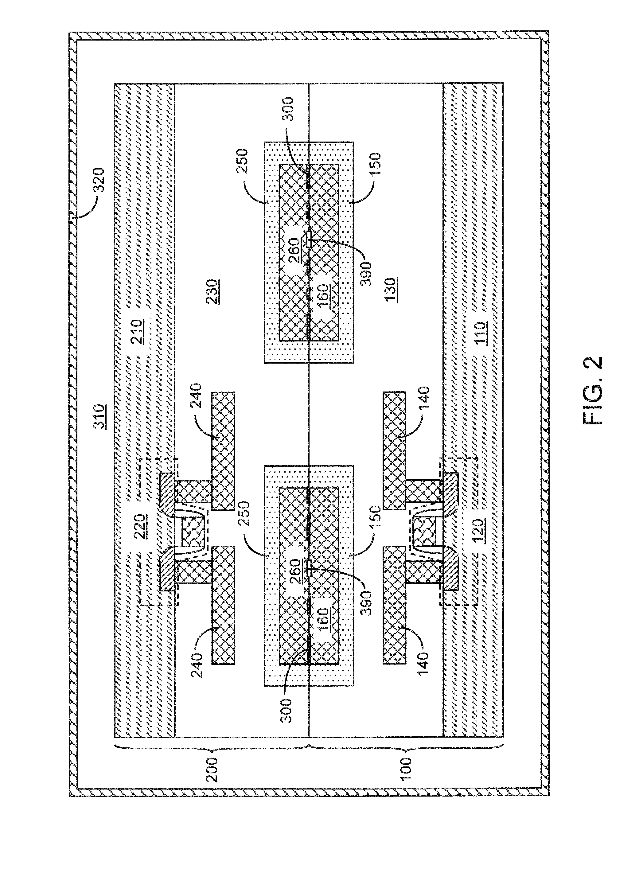
[0028]Referring to FIG. 1, a first exemplary structure according to the present invention includes a first substrate 100 and a second substrate 200 facing each other. The first substrate 100 can include a first semiconductor substrate 110 and at least one first dielectric material layer 130 located thereupon. The second substrate 200 can include a second semiconductor substrate 210 and at least one second dielectric material layer 230 located thereupon. Each of the first and second semiconductor substrates (110, 210), if present, comprises a semiconductor material, which may be selected from, but is not limited to, silicon, germanium, silicon-germanium alloy, silicon carbon alloy, silicon-germanium-carbon alloy, gallium arsenide, indium arsenide, indium phosphide, III-V compound semiconductor materials, II-VI compound semiconductor materials, organic semiconductor materials, and other compound semiconductor materials. For example, the semiconductor material can be silicon. Each of t...

second embodiment

[0049]Referring to FIG. 4, a second exemplary structure according to the present invention includes a first substrate 100 and a second substrate 200, each of which can the same as the first substrate 100 and the second substrate 200, respectively, in the first exemplary structure of FIG. 1 as described above.

[0050]Before the first substrate 100 and the second substrate 200 are brought into physical contact, the first surface(s) 161 of the at least one first metal pad 160 is / are recessed by a recess depth Rd relative to the first dielectric surface 131 of the at least one first dielectric material layer 130. The recess depth Rd can be from 5 nm to 3,000 nm, and typically from 30 nm to 300 nm, although lesser and greater recess depths can also be employed.

[0051]After recessing the first surface(s) 161 of the at least one first metal pad 160, the first substrate 100 and the second substrate 200 are brought into physical contact with each other in the same manner as in the first embodim...

third embodiment

[0059]Referring to FIG. 7, a third exemplary structure according to the present invention includes a first substrate 100 and a second substrate 200, each of which can the same as the first substrate 100 and the second substrate 200, respectively, in the first exemplary structure of FIG. 1 as described above.

[0060]Before the first substrate 100 and the second substrate 200 are brought into physical contact, the first surface(s) 161 of the at least one first metal pad 160 is / are recessed by a recess depth Rd relative to the first dielectric surface 131 of the at least one first dielectric material layer 130 as in the second embodiment. In addition, before the first substrate 100 and the second substrate 200 are brought together, the second surface(s) 261 of the at least one second metal pad 260 is / are recessed by another recess depth Rd′ relative to the second dielectric surface 231 of the at least one second dielectric material layer 230. The recess depths Rd and Rd′ can be from 5 nm...


PUM


Abstract

Two substrates are brought together and placed in a plating bath. In one embodiment, a conductive material is plated in microscopic cavities present at the interface between a first metal pad and a second metal pad to form at least one interfacial plated metal liner portion that adheres to a surface of the first metal pad and a surface of the second metal pad. In another embodiment, at least one metal pad is recessed relative to a dielectric surface before being brought together. The two substrates are placed in a plating bath and a conductive material is plated in the cavity between the first metal pad and the second metal pad to form a contiguous plated metal liner layer that adheres to a surface of the first metal pad and a surface of the second metal pad.

Description

BACKGROUND[0001]This invention relates to bonded structures including a self-aligned liner that bonds metal pads located on each side of bonded substrates and methods of manufacturing the same.[0002]Bonding of multiple substrates is required to enable three-dimensional integration of chips. Bonding of two substrates can be effected by adhesion between two dielectric materials as in an oxide-to-oxide bonding that fuses silicon dioxide materials from two substrates after bonding, by adhesion between two metallic materials as in a copper-to-copper bonding that employs direct contact between two copper pads and a subsequent grain growth across the original interface between the two copper pads, or by a method employing a combination of the two adhesion mechanisms.[0003]The effectiveness of currently available bonding methods is limited by the bonding strength, i.e., the mechanical adhesion strength, between the two substrates that are bonded together. Because substrates including semico...

Claims


Application Information

Patent Timeline
IPC IPC(8): H01L23/488H01L21/50
CPCH01L24/03H01L24/05H01L2924/1305H01L2924/1306H01L2224/08121H01L24/08H01L24/80H01L25/50H01L2224/80001H01L2224/80359H01L2225/06513H01L2924/01029H01L2924/0103H01L2924/01049H01L2924/01073H01L2924/01079H01L2924/01005H01L2924/01006H01L2924/01019H01L2924/01023H01L2924/01024H01L2924/01033H01L2924/01044H01L2924/01045H01L2924/01047H01L2924/0105H01L2924/01074H01L2924/01077H01L2224/05554H01L2224/0556H01L2224/05099H01L2224/0502H01L2224/05014H01L2224/05599H01L2224/80345H01L2224/80357H01L2224/80895H01L2224/80896H01L2924/00H01L2224/821H01L24/82H01L24/92H01L2224/9212H01L2224/05547H01L2224/05007H01L2224/05571H01L2224/05557H01L2224/80986H01L2224/8034H01L2224/08501H01L2224/08145H01L2224/80H01L2224/82
Inventor YANG, CHIH-CHAOHORAK, DAVID V.NOGAMI, TAKESHIPONOTH, SHOM
Owner TAIWAN SEMICON MFG CO LTD
Why Eureka
Try Eureka