Display device and touch panel device

Active Publication Date: 2019-04-18
JAPAN DISPLAY INC
View PDF13 Cites 8 Cited by
  • Summary
  • Abstract
  • Description
  • Claims
  • Application Information

AI Technical Summary

Benefits of technology

[0005]In order to reduce electromagnetic interference (EMI) due to the drive waveform on the transmission side in driving the electrostatic capacitance touch panel device, the inventors have investigated a technique for the purpose of mitiga

Problems solved by technology

However, in this method, it is found that the size of the touch panel device is likely increased beca

Method used


Image

  • Display device and touch panel device
  • Display device and touch panel device
  • Display device and touch panel device

Examples


embodiment

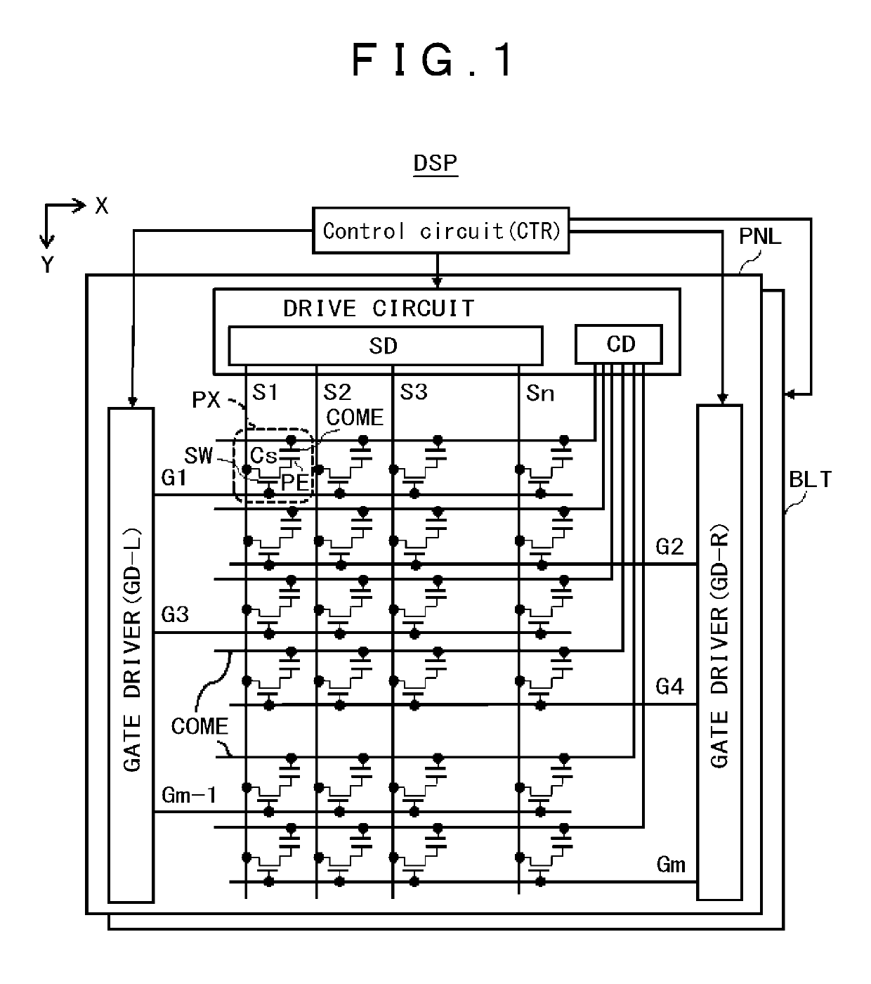
[0037]FIG. 1 is a diagram of a schematic configuration of a display device DSP equipped with a sensor according to an embodiment. Note that, in the embodiment, the display device is a liquid crystal display device.

[0038]The display device DSP equipped with a sensor includes a display panel PNL and a backlight BLT that illuminates the display panel PNL from the back face side. The display panel PNL is provided with a display unit including display pixels PX disposed in a matrix configuration.

[0039]As shown in FIG. 1, the display unit includes gate lines G (G1, G2 . . . ) along which a plurality of display pixels PX are arrayed extending along the rows of the lines G, source lines S (S1, S2 . . . ) along which the display pixels PX is arrayed extending along the columns of the liens S, and pixel switches SW individually disposed near locations at which the gate line G, which is a scanning line, crosses the source line S, which is a signal line. The display pixels PX each have a pixel ...


PUM


Abstract

There is provided a display device equipped with a touch sensor that can decrease the area of the mounting surface with electromagnetic interference reduced. The display device includes a plurality of drive electrodes, an output circuit connected to the plurality of drive electrodes, a power supply circuit, and a resistor element. A power of the output circuit is connected to the power supply circuit through the resistor element.

Description

CROSS-REFERENCE TO RELATED APPLICATIONS[0001]The present application claims priority from Japanese Patent Application JP 2017-201712 filed on Oct. 18, 2017, the content of which is hereby incorporated by reference into this application.BACKGROUND OF THE INVENTION[0002]The present invention relates to a display device that is specifically applicable to a display device equipped with a touch sensor.[0003]In addition to a so-called on-cell type display device in which a touch panel is formed on the display surface of the display device, display devices below are proposed as display devices equipped with a touch sensor: a so-called in-cell type display device in which a display common electrode that is originally provided on the display device is shared as one (a drive electrode Tx) of paired touch sensor electrodes, the other electrode (a detection electrode Rx) is disposed crossing this common electrode, and the drive electrode Tx and the detection electrode Rx are integrated into the...

Claims


Application Information

Patent Timeline
IPC IPC(8): G06F3/041G06F3/044
CPCG06F3/0416G06F3/044G06F3/0412G06F2203/04107G06F2203/04102G06F3/04166G06F3/04164G06F3/0446
Inventor TANAKA, TOSHIHIKOTAKADA, NAOKITANAKA, CHIHIRO
Owner JAPAN DISPLAY INC
Why Eureka
Try Eureka