
Selective shallow trench isolation (STI) fill for stress engineering in semiconductor structures

Active Publication Date: 2019-05-02
GLOBALFOUNDRIES US INC
View PDF8 Cites 1 Cited by
  • Summary
  • Abstract
  • Description
  • Claims
  • Application Information

AI Technical Summary

Benefits of technology

This patent describes a structure and method for creating a single diffusion break (SDB) region in a semiconductor device. The SDB region includes a shallow trench isolation (STI) region with a stress fill material within a recess of the STI region, which imparts a stress on a nearby gate structure. The technical effect of this structure and method is that it helps improve the performance and reliability of the semiconductor device, particularly by enhancing the stability and reliability of the gate structure.

Problems solved by technology

However, the use of such DDB isolation structures consumes more of the available space on a substrate than does the use of SDB isolation structures, thereby leading to reduced packing densities.
Moreover, SDB device performance is weaker compared to DDB devices.
The weaker device performance of SDB devices restricts its usage in the chip even though it has higher packaging density than DDB devices.
Moreover, faceted source / drain poses another problem while trying to boost SDB device performance, particularly using junction elements.
For example, faceted source / drain in SDB devices can lead to approximately an 8-10% performance gap compared to DDB devices because the source / drain is not fully grown in the facet.

Method used


Image

  • Selective shallow trench isolation (STI) fill for stress engineering in semiconductor structures
  • Selective shallow trench isolation (STI) fill for stress engineering in semiconductor structures
  • Selective shallow trench isolation (STI) fill for stress engineering in semiconductor structures

Examples


Embodiment Construction

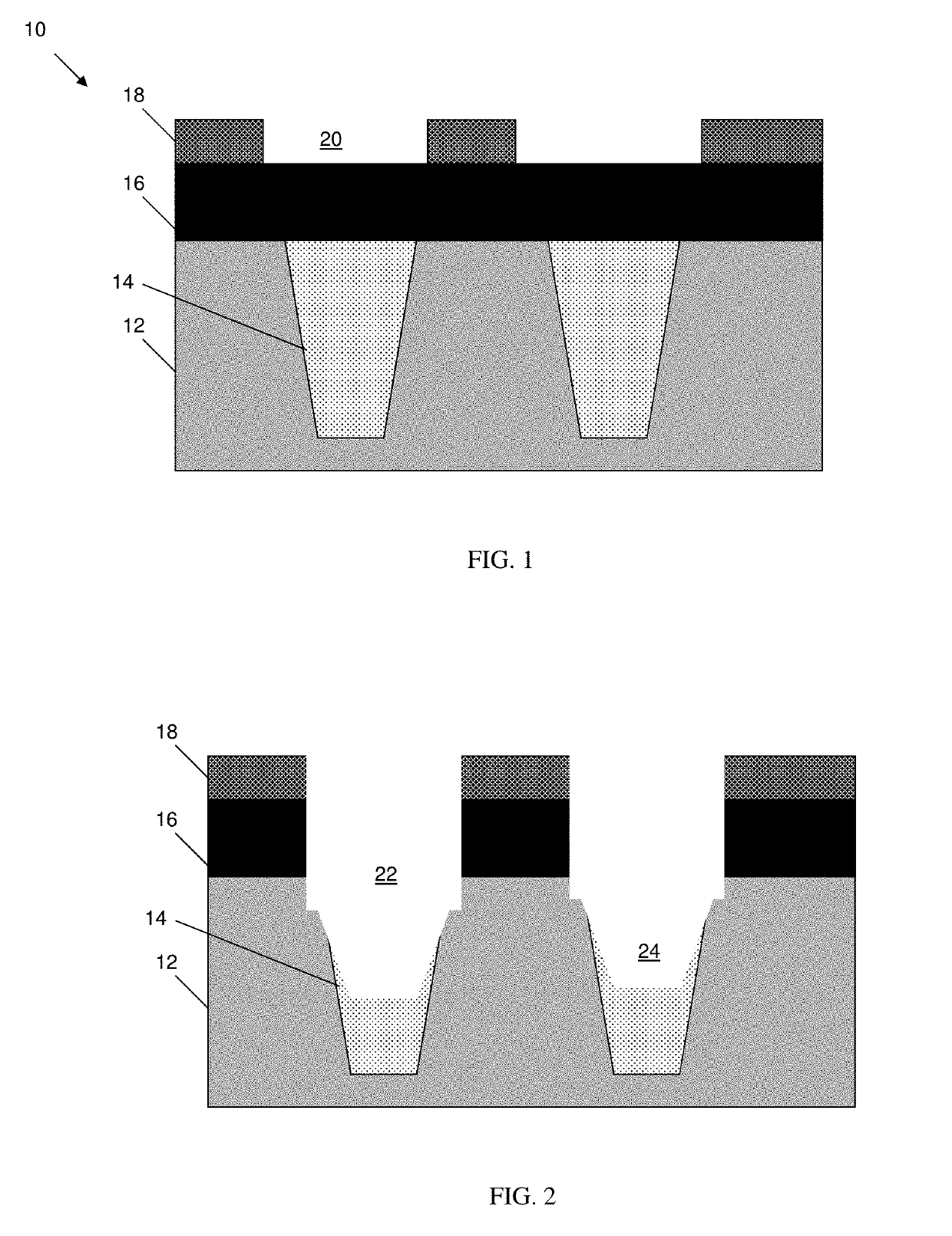
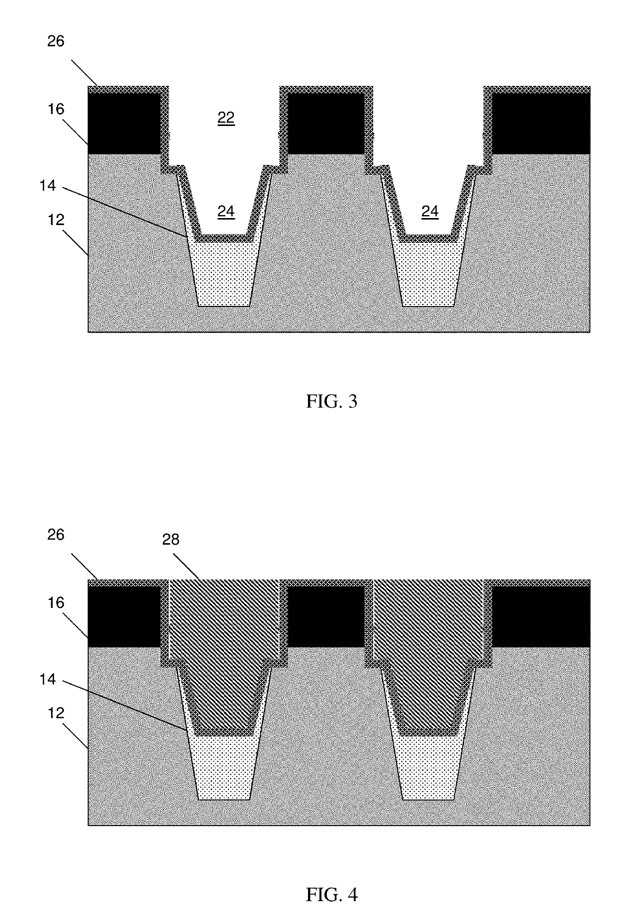
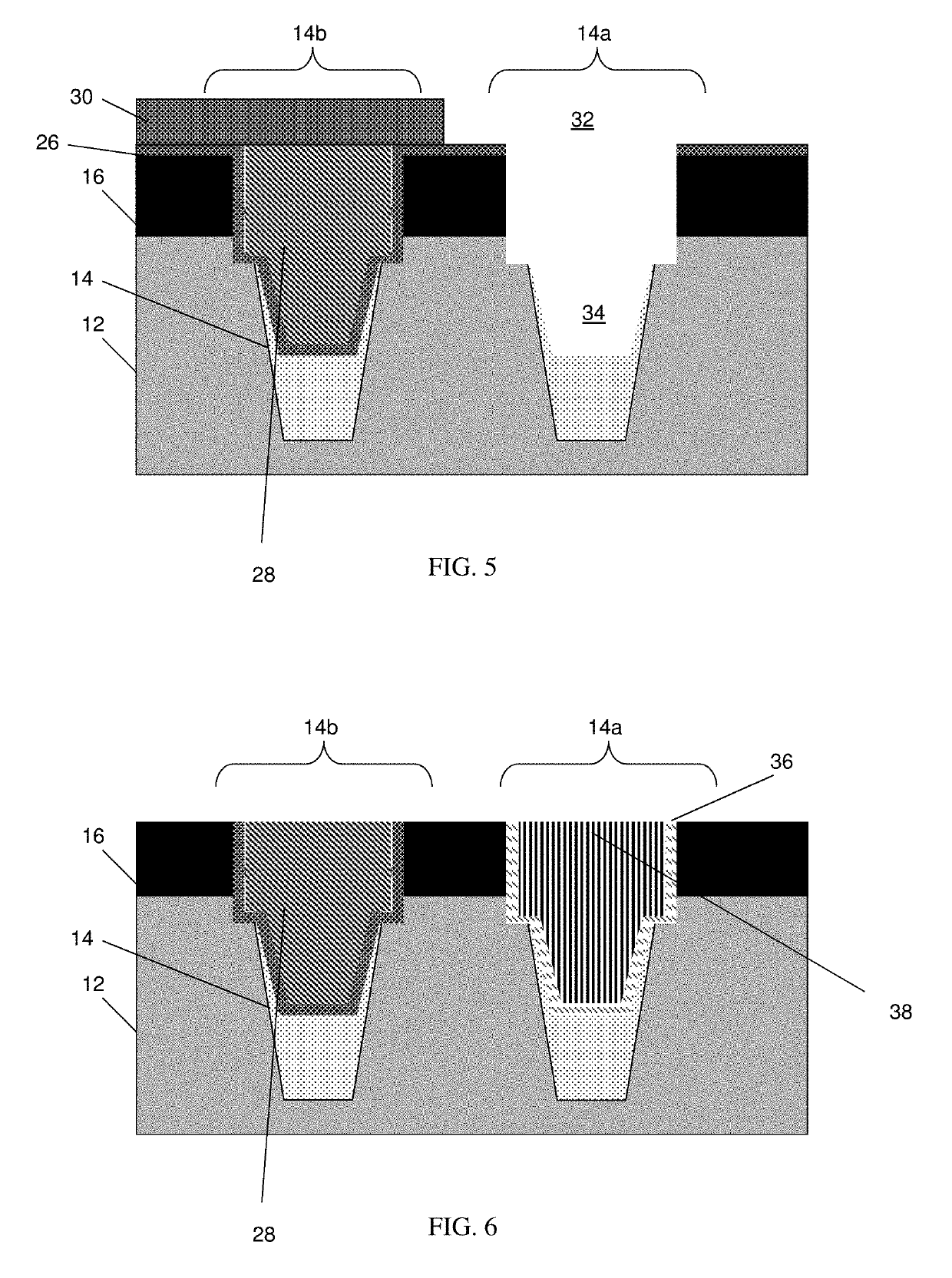
[0017]The present disclosure relates to semiconductor structures and, more particularly, to selective shallow trench isolation (STI) fill material for stress engineering in semiconductor structures and methods of manufacture. More specifically, the present disclosure relates to STI fill material for stress engineering in single diffusion break (SDB) devices and methods of manufacture. Advantageously, the present disclosure provides improved SDB NFET / PFET performance using strain engineering while not affecting double diffusion break (DDB) device performance.

[0018]In embodiments, the STI fill material is provided near the SDB device to induce favorable stress in SDB NFET devices and SDB PFET devices, while having no impact on the DDB devices. That is, in embodiments, while making changes to the SDB STI, e.g., providing stress engineering, the DDB devices are masked by thick masking material, e.g., SiN layer, hence preventing any impact on the DDB region. The STI fill material can inc...


PUM


Abstract

The present disclosure relates to semiconductor structures and, more particularly, to selective shallow trench isolation (STI) fill material for stress engineering in semiconductor structures and methods of manufacture. The structure includes a single diffusion break (SDB) region having at least one shallow trench isolation (STI) region with a stress fill material within a recess of the at least one STI region. The stress fill material imparts a stress on a gate structure adjacent to the at least one STI region.

Description

FIELD OF THE INVENTION[0001]The present disclosure relates to semiconductor structures and, more particularly, to selective shallow trench isolation (STI) fill for stress engineering in semiconductor structures and methods of manufacture.BACKGROUND[0002]In a double diffusion break (DDB) structure, a lateral width (in the current transport direction or gate length direction of the FinFET devices) of the isolation material between two active regions approximately corresponds to the lateral width of two of the gate structures. On the other hand, in a single diffusion break (SDB), the lateral width (in the current transport direction or gate length direction of the FinFET devices) of the isolation material between the two active regions is less than the lateral width of a single gate structure.[0003]In general, it is easier to form a DDB isolation structure than it is to form a SDB due to the relatively larger size of the DDB isolation structure. However, the use of such DDB isolation s...

Claims


Application Information

Patent Timeline
IPC IPC(8): H01L29/78H01L29/06H01L27/092H01L21/762H01L21/8238
CPCH01L29/7846H01L29/0649H01L27/0922H01L21/76224H01L21/823878H01L27/0924H01L21/823821H01L21/823828H01L21/3081H01L21/3065H01L21/31116H01L29/66545H01L21/823807H01L29/66795
Inventor JHA, ASHISH KUMARYU, HONGDOU, XINYUANWU, XUSHENGCHOI, DONGILBANGHART, EDMUND K.HASSAN, MD KHALED
Owner GLOBALFOUNDRIES US INC
Learn More