Active Fixed Beam Antenna Array

a fixed beam antenna and high gain technology, applied in the direction of individually energised antenna arrays, resonant antennas, protective materials radiating elements, etc., can solve the problems of rf transmission loss, ordinary dielectric materials such as rfb>4/b>, and cannot meet the requirements for so as to minimize the loss of radio frequency (rf) transmission, and reduce the length of the connection

Active Publication Date: 2019-05-23
AVL TECH
View PDF0 Cites 2 Cited by
  • Summary
  • Abstract
  • Description
  • Claims
  • Application Information

AI Technical Summary

Benefits of technology

[0005]In accordance with one form of the present invention, there is provided a fixed beam high gain antenna for generating high gain for satellite communication ground terminals, the antenna including a multi-layer printed circuit board (PCB) having a top surface forming a rear surface of the antenna and a bottom layer forming a front surface of the antenna; an antenna array including a plurality of antenna patches on the front surface of the antenna and a plurality of application-specific integrated circuits (ASICs) on the rear surface of the antenna; wherein the antenna array comprises at least one antenna unit cell each including one of the plurality of ASICs in connection with a corresponding plurality of the plurality of antenna patches; wherein each one of the plurality of ASICs is centrally positioned and surrounded by the corresponding plurality of antenna patches; and wherein a reduced length of the connection between each of the plurality of ASICs and the corresponding plurality of antenna patches minimizes radio frequency (RF) transmission loss.
[0006]In accordance with another form of the present invention, there is provided a fixed beam high gain antenna for generating high gain for satellite communication ground terminals, the antenna including a multi-layer printed circuit board (PCB) having a top surface forming a rear surface of the antenna and a bottom layer forming a front surface of the antenna; a plurality of TX patches and a plurality of RX patches on the front surface of the antenna; a plurality of TX application-specific integrated circuits (ASICs) and a plurality of RX ASICs on the antenna rear surface; an antenna array including a plurality of TX patches and a plurality of RX patches on the front surface of the antenna and a plurality of TX application-specific integrated circuits (ASICs) and a plurality of RX ASICs on the rear surface of the antenna; wherein the antenna array comprises at least one TX unit cell each including one of the plurality of TX ASICs in connection with a corresponding four of the plurality of TX patches and an RX unit cell each including one of the plurality of RX ASICs in connection with a corresponding four of the plurality of RX patches; wherein each one of the plurality of TX ASICs is centrally positioned and surrounded by the corresponding four TX patches and each one of the plurality of RX ASICs is centrally positioned and surrounded by the corresponding four RX patches; and wherein a reduced length of the connection between each of the plurality of TX ASICs and the corresponding plurality of TX patches and between each of the plurality of RX ASICs and the corresponding plurality of RX patches minimizes RF transmission loss.
[0007]In accordance with another form of the present invention, there is provided a fixed beam high gain antenna for generating high gain for satellite communication ground terminals, the antenna including a multi-layer printed circuit board (PCB) having a top surface forming a rear surface of the antenna and a bottom layer forming a front surface of the antenna; a hybrid antenna array including a plurality of TX patches and a plurality of RX patches on the front surface of the antenna and a plurality of TX application-specific integrated circuits (ASICs) and a plurality of RX ASICs located on the rear surface of the antenna; wherein each of the plurality of RX patches on the front surface of the antenna is centrally positioned and surrounded by four TX patches on the front surface of the antenna; wherein each of the plurality of TX ASICs on the rear surface of the antenna is surrounded by and in connection with a corresponding four TX patches of the plurality of TX patches on the front surface of the antenna; wherein each of the plurality of RX ASICs on the rear surface of the antenna is surrounded by and in connection with a corresponding four RX patches of the plurality of RX patches on the front surface of the antenna; and wherein a first reduced length of the connection between each one of the plurality of TX ASIC and the corresponding four TX patches and a second reduced length of the connection between each one of the plurality of RX ASIC and the corresponding four RX patches minimizes RF transmission loss.

Problems solved by technology

For satellite communications, the ordinary dielectric material, such as RF4, cannot meet the requirement for radio frequency (RF) transmission due to non-negligible loss at high frequency.
Even if specialized high-frequency dielectric material is used for RF feed, the RF transmission loss is noticeable, particularly at Ka band frequencies (20-30 GHz).

Method used


Image

  • Active Fixed Beam Antenna Array
  • Active Fixed Beam Antenna Array
  • Active Fixed Beam Antenna Array

Examples


Embodiment Construction

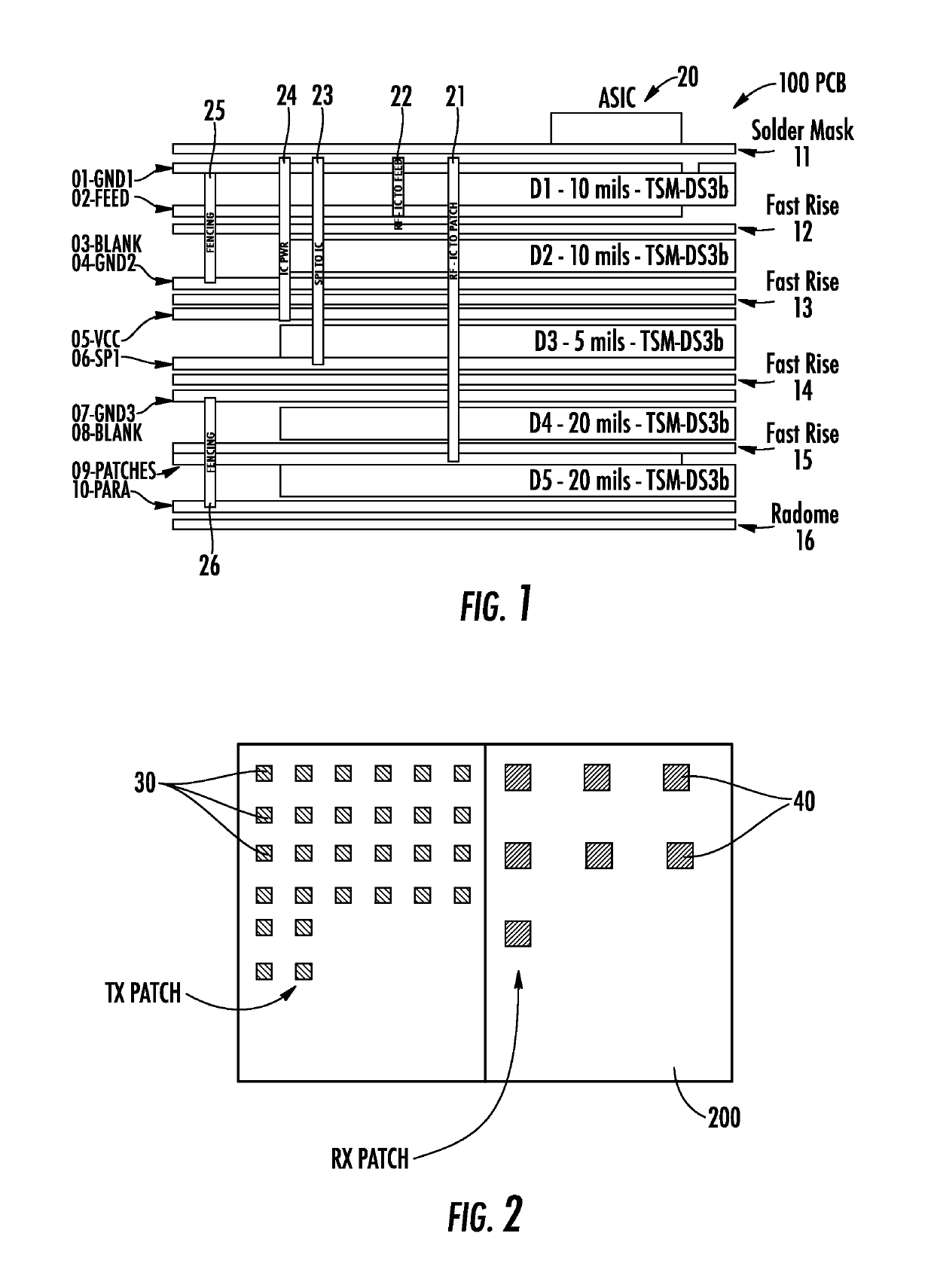
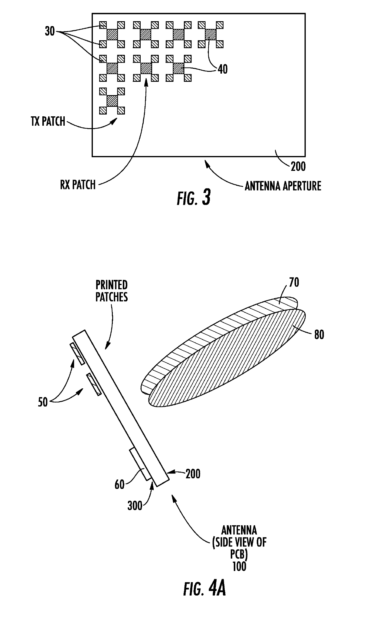
[0018]In the present invention, a novel fixed beam high gain antenna array composed of antenna patches and their corresponding application-specific integrated circuits (ASICs) is utilized to generate high gain of a fixed beam for satellite communication ground terminals. The antenna patches include TX and RX patches that are located within the bottom layer of a multi-layer printed circuit board (PCB). The corresponding TX and RX ASICs are located on the top surface of the PCB. Four antenna patches are connected to one corresponding ASIC through PCB transmission lines and signal vias, forming one unit cell. In one preferred embodiment, the ratio of TX to RX patches is 4:1. Within the bottom layer of the PCB, one RX patch is surrounded by four TX patches and the four TX patches are placed as close as possible to the one RX patch. Additionally, one TX ASIC located on the top surface of the PCB corresponds to four TX patches within the bottom layer of the PCB, forming a TX unit cell. Li...


PUM


Abstract

A fixed beam high gain antenna for generating high gain for satellite communication ground terminals includes a multi-layer PCB having a top surface forming a rear surface of the antenna and a bottom layer forming a front surface of the antenna; an antenna array including a plurality of antenna patches on the front surface of the antenna and a plurality of application-specific integrated circuits (ASICs) on the rear surface of the antenna; wherein the antenna array comprises at least one antenna unit cell each including one of the plurality of ASICs in connection with a corresponding plurality of the plurality of antenna patches; wherein each one of the plurality of ASICs is centrally positioned and surrounded by the corresponding plurality of antenna patches; and wherein a reduced length of the connection between each of the plurality of ASICs and the corresponding plurality of antenna patches minimizes RF transmission loss.

Description

RELATED APPLICATION[0001]This application claims priority to and incorporates entirely by reference U.S. Provisional Patent Application Ser. No. 62 / 581,168 filed on Nov. 3, 2017.FIELD OF THE INVENTION[0002]This invention relates to a fixed beam high gain antenna array containing antenna patches and integrated circuits (ICs) within which solid-state power amplifiers (SSPAs) are embedded. Particularly, this invention presents an array in which the antenna patches (TX and RX patches) are located on one side of the printed circuit board (PCB), while their corresponding application-specific integrated circuits (ASICs) are located on the opposite side of the PCB. Thus, the antenna patches can be arranged as close as possible to each other and generate high gain at a fixed beam.BACKGROUND OF THE INVENTION[0003]A fixed beam antenna is a directional antenna steered to one desired direction, ideally generating the highest gain in the main lobe without any side lobes. For satellite communicati...

Claims


Application Information

Patent Timeline
Patent Type & Authority Applications(United States)
IPC IPC(8): H01Q21/06H01Q9/04H01Q23/00H01Q1/52H01Q1/22H01Q1/28
CPCH01Q21/065H01Q9/0407H01Q23/00H01Q1/523H01Q1/22H01Q1/288H01Q1/38H01Q1/40H01Q25/007H01Q1/28H01Q1/52H01Q9/04
Inventor TIMMINS, IAN J.EDENFIELD, KEITHBARRATT, BRUCEELLIS, ALAN
Owner AVL TECH
Why Eureka
Try Eureka