
Electronic component

Active Publication Date: 2019-05-30
TDK CORPARATION
View PDF11 Cites 5 Cited by
  • Summary
  • Abstract
  • Description
  • Claims
  • Application Information

AI Technical Summary

Benefits of technology

The patent text describes a technology that prevents electronic components from cracking and getting bigger when they are solder-mounted on electronic devices. This is achieved by using a conductive resin layer that absorbs stress and protects the component from external force. The technology results in smaller components and reduces the likelihood of cracks.

Problems solved by technology

In this case, a crack may occur in the element body.
Therefore, it may be difficult to sufficiently obtain the effect of suppressing a crack in the element body without increasing the size of the electronic component.

Method used


Image

  • Electronic component
  • Electronic component
  • Electronic component

Examples


Embodiment Construction

[0027]Hereinafter, embodiments of the present invention will be described in detail with reference to the accompanying drawings. In the following description, the same elements or elements having the same functions are denoted with the same reference numerals and overlapped explanation is omitted.

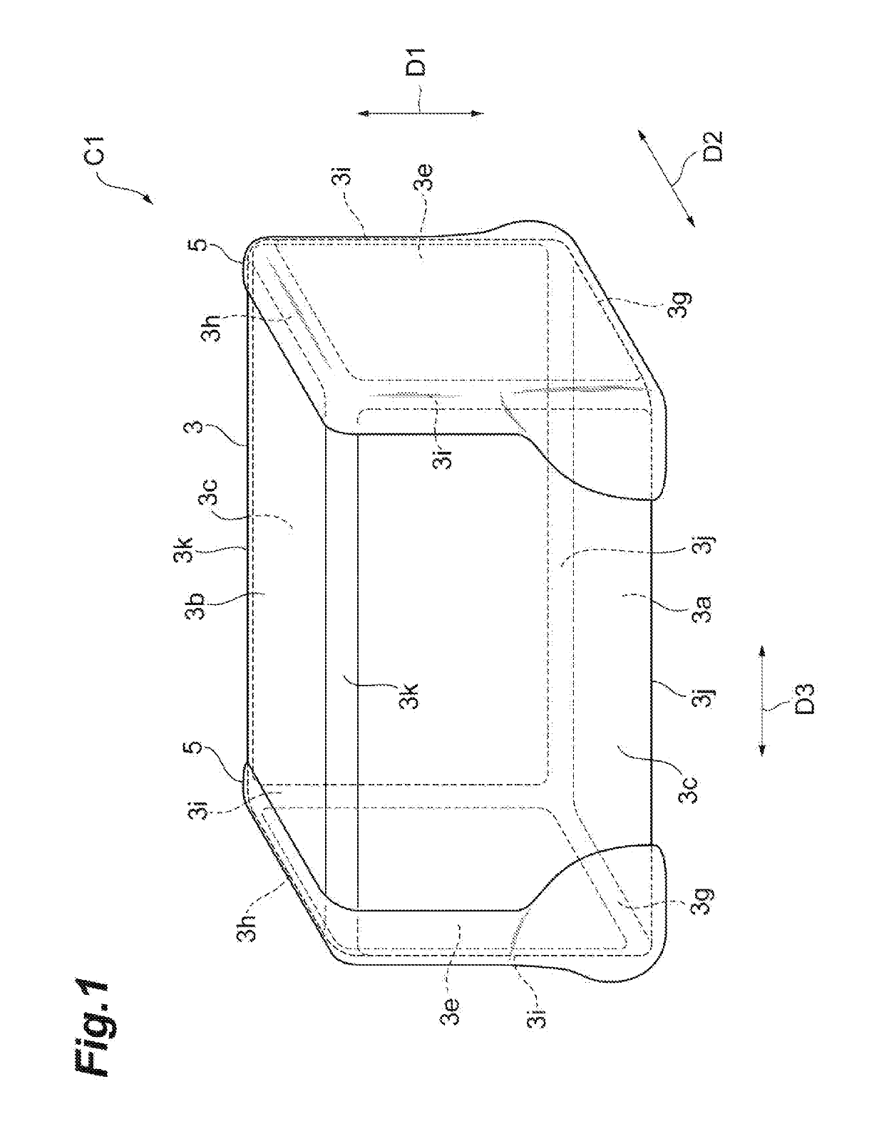
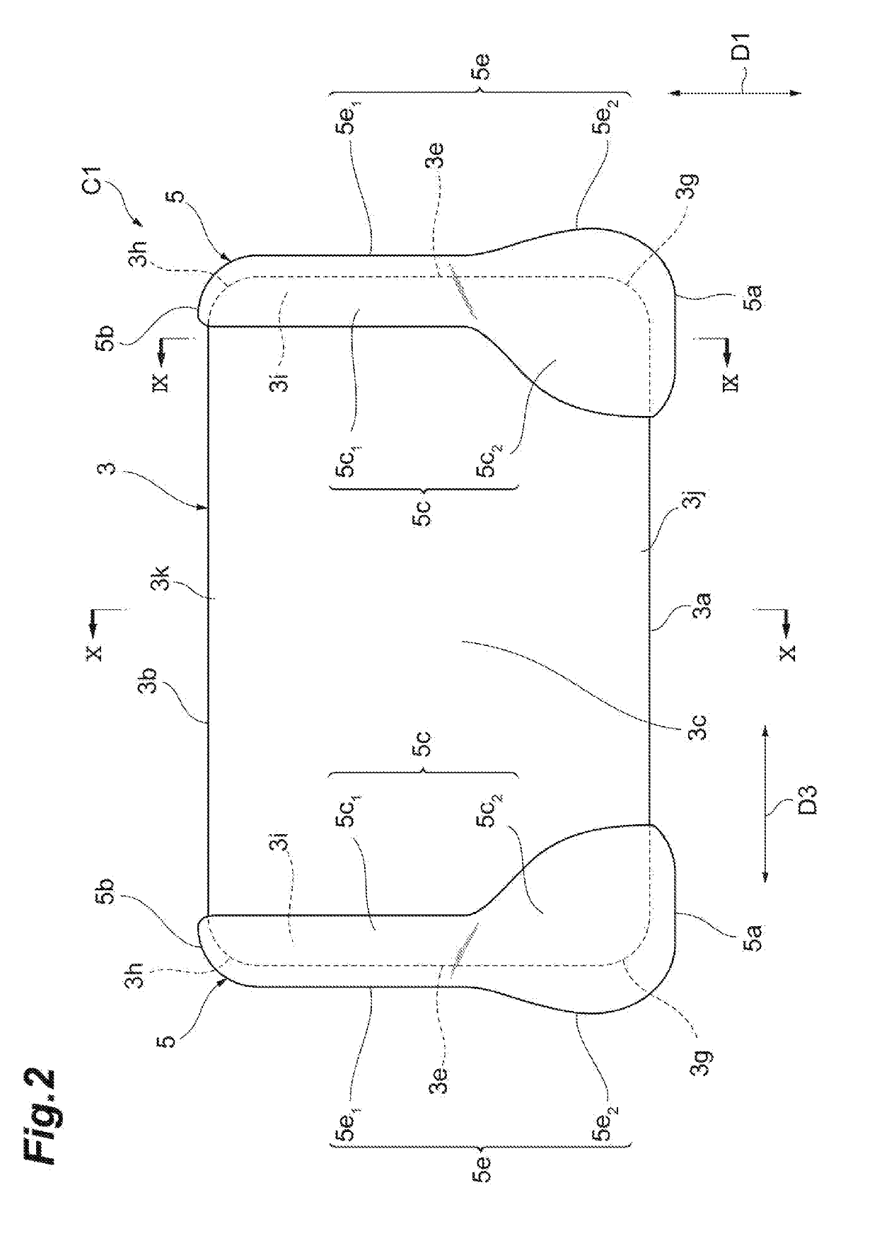
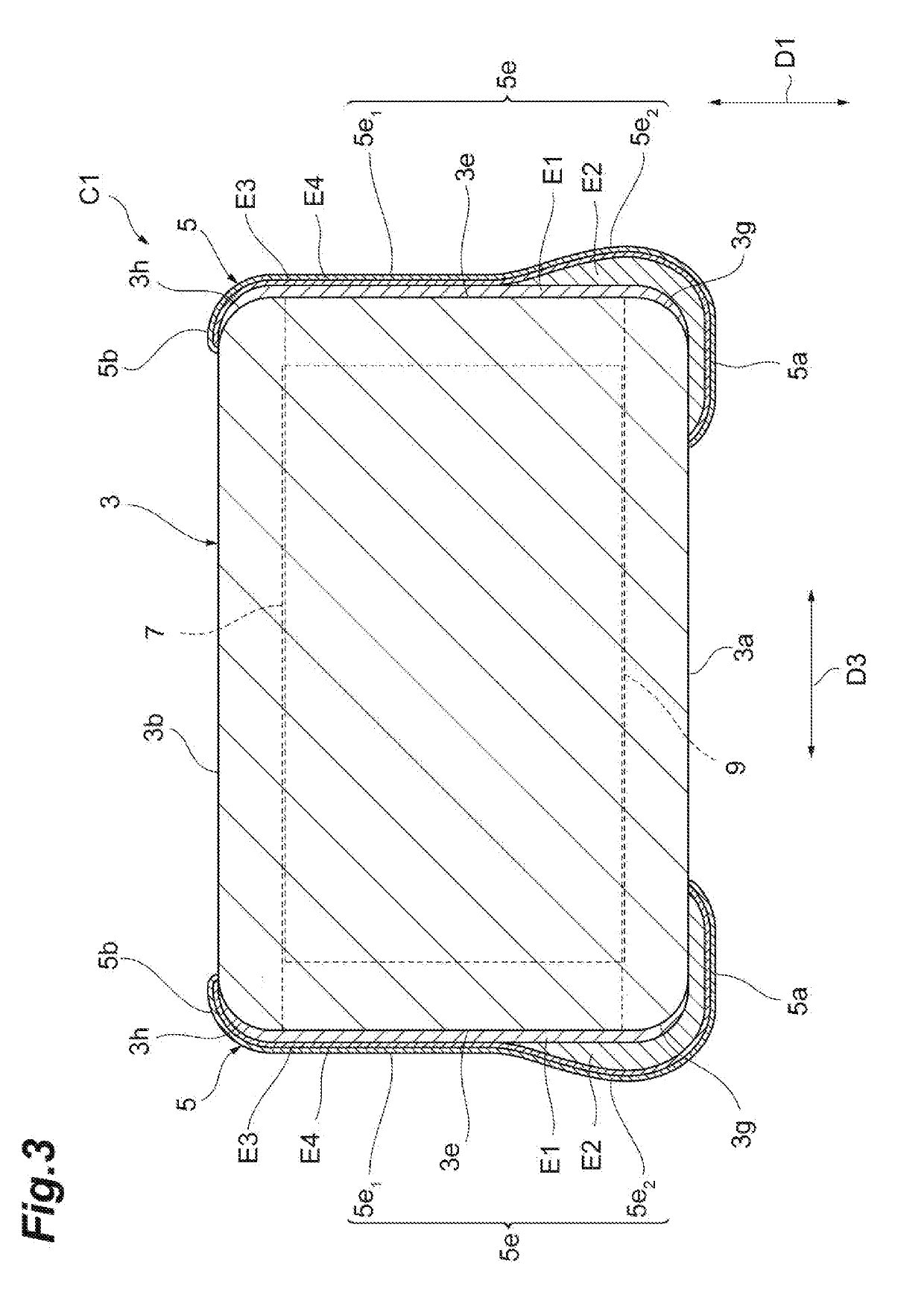
[0028]A configuration of a multilayer capacitor C1 according to an embodiment will be described with reference to FIGS. 1 to 8. FIG. 1 is a perspective view of the multilayer capacitor according to the embodiment. FIG. 2 is a side view of the multilayer capacitor according to the embodiment. FIGS. 3 to 5 are views illustrating a cross-sectional configuration of the multilayer capacitor according to the embodiment. FIG. 6 is a plan view illustrating an element body, a first electrode layer, and a second electrode layer. FIG. 7 is a side view illustrating the element body, the first electrode layer, and the second electrode layer. FIG. 8 is an end view illustrating the element body, the first...


PUM

PropertyMeasurementUnit
Lengthaaaaaaaaaa
Shapeaaaaaaaaaa
Electrical conductoraaaaaaaaaa

Abstract

An element body of a rectangular parallelepiped shape includes a pair of principal surfaces opposing each other in a first direction, a pair of side surfaces opposing each other in a second direction, and a pair of end surfaces opposing each other in a third direction. An external electrode disposed on an end portion of the element body in the third direction. When viewed from the third direction, a width of the element body in the second direction is the largest at a central position in the first direction, and gradually decreases from the central portion in the first direction. When viewed from the third direction, a position in which a length from one end to another end of the conductive resin layer in the second direction is the largest is located closer to the one principal surface than the central position.

Description

BACKGROUND OF THE INVENTION1. Field of the Invention[0001]The present invention relates to an electronic component.2. Description of Related Art[0002]Known electronic components include an element body of a rectangular parallelepiped shape and a plurality of external electrodes (see, for example, Japanese Unexamined Patent Publication No. H8-107038). The element body includes a pair of principal surfaces opposing each other, a pair of end surfaces opposing each other, and a pair of side surfaces opposing each other. The plurality of external electrodes is disposed at each end portion of the element body in a direction in which the pair of end surfaces opposes each other. The external electrode includes a conductive resin layer.SUMMARY OF THE INVENTION[0003]In a case in which the electronic component is solder-mounted on an electronic device, external force applied onto the electronic component from the electronic device may act as stress on the element body. The electronic device in...

Claims


Application Information

Patent Timeline
IPC IPC(8): H01G4/30H01G4/008H01G4/12
CPCH01G4/30H01G4/008H01G4/1227H01G4/005H01G4/232
Inventor ONODERA, SHINYATAMURA, TAKEHISAMORITA, KENTAKEDA, ATSUSHI
Owner TDK CORPARATION
Learn More