Semiconductor device

Active Publication Date: 2019-06-06
SAMSUNG ELECTRONICS CO LTD
View PDF13 Cites 0 Cited by
  • Summary
  • Abstract
  • Description
  • Claims
  • Application Information

AI Technical Summary

Benefits of technology

This patent describes a semiconductor device that can improve memory performance by using information about expiration time for data. By performing operations on the memory device at the right time, the device can secure more capacity and optimize garbage collection.

Problems solved by technology

Such flash-based storage devices do not perform data operations on a single memory cell at a time due to the characteristics of a memory device.

Method used


Image

  • Semiconductor device
  • Semiconductor device
  • Semiconductor device

Examples


Embodiment Construction

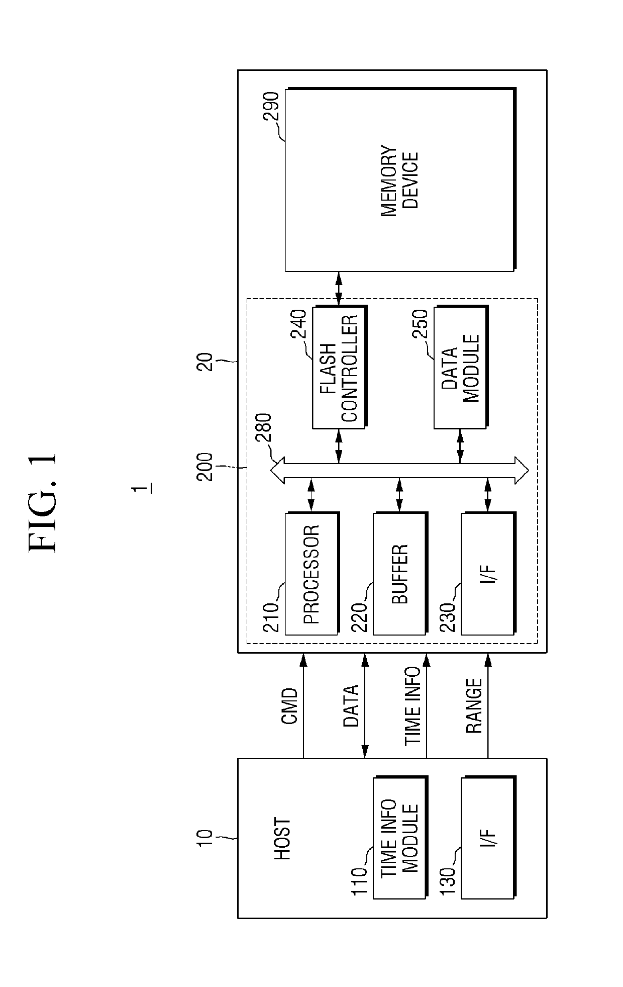
[0026]FIG. 1 is a block diagram of an embodiment of a semiconductor system 1.

[0027]Referring to FIG. 1, semiconductor system 1 may include a host 10 and a storage device 20.

[0028]Host 10 may request data to be stored in storage device 20 or request data to be read from storage device 20. For example, host 10 may transmit a data write command CMD and data DATA to be written to storage device 20 through a host interface (1 / F) 130. In addition, host 10 may transmit a data read command CMD to storage device 20 and receive read data DATA from storage device 130 through host interface 130.

[0029]Host 10 may exchange commands CMD and data DATA with storage device 20 according to an interface supported by storage device 20. In some embodiments, examples of protocols or standards to which the interface between host 10 and storage device 20 may conform include Universal Flash Storage (UFS), Small Computer System Interface (SCSI), Serial Attached SCSI (SAS), Serial Advanced Technology Attachmen...


PUM


Abstract

A semiconductor device includes: a memory device; and a storage controller. The storage controller includes a flash controller performing data operations on the memory device, and a processor executing a real-time operating system (RTOS) for controlling the flash controller, wherein the RTOS receives expiration time information of data from a host and performs at least one of the data operations using a scheduler based on the expiration time information.

Description

[0001]This application claims the benefit of Korean Patent Application No. 10-2017-0166817, filed on Dec. 6, 2017, in the Korean Intellectual Property Office, the disclosure of which is incorporated herein in its entirety by reference.BACKGROUND1. Field of the Disclosure[0002]The present disclosure relates to a semiconductor device, and more particularly, to a semiconductor device which performs data operations on a memory device.2. Description of the Related Art[0003]Various flash memory-based storage devices perform various data operations on a memory device. For example, after receiving a command to read or write data from a host, a storage device may perform various data operations such as read, write, program, and erase operations to process the command.[0004]Such flash-based storage devices do not perform data operations on a single memory cell at a time due to the characteristics of a memory device. For example, read and write operations may be performed on a page-by-page bas...

Claims


Application Information

Patent Timeline
IPC IPC(8): G06F3/06
CPCG06F3/0659G06F3/0604G06F3/0679G06F3/0608G06F3/064G06F2212/7205G06F2212/7201G06F12/0246G06F2212/7204G06F2212/1016G06F12/0253
Inventor KIM, JUNG HOONLEE, YOUNG-SIKROH, KANG HO
Owner SAMSUNG ELECTRONICS CO LTD
Why Eureka
Try Eureka