Packaging method and package structure of qled device

Active Publication Date: 2019-06-20
SHENZHEN CHINA STAR OPTOELECTRONICS SEMICON DISPLAY TECH CO LTD
View PDF2 Cites 3 Cited by
  • Summary
  • Abstract
  • Description
  • Claims
  • Application Information

AI Technical Summary

Benefits of technology

[0037]The beneficial effects of the present disclosure are as follows: the method for packaging a QLED device provided by the present disclosure forms a thin film encapsulation layer in which a plurality of inorganic barrier layers and at least one organic buffer layer are alternately stacked on a QLED device to seal the QLED device against water and oxygen, and the organic buffer layer is further doped with a thermal conducting material, so that the heat generated by the QLED device can be promptly transmitted through the thin film encapsulation layer to improve the heat dissipation of the thin film encapsulation layer, thereby improving the light extraction efficiency and th

Problems solved by technology

However, the QLED device is very sensitive to water and oxygen, and is highly susceptible to water and oxygen in the surrounding environment to cause device failure.
However, the high hermetic package structure will lead to the devi

Method used


Image

  • Packaging method and package structure of qled device
  • Packaging method and package structure of qled device

Examples


Example

[0043]To further illustrate the technical means adopted by the present disclosure and the effects thereof, the following describes in detail the preferred embodiments of the present disclosure and the accompanying drawings.

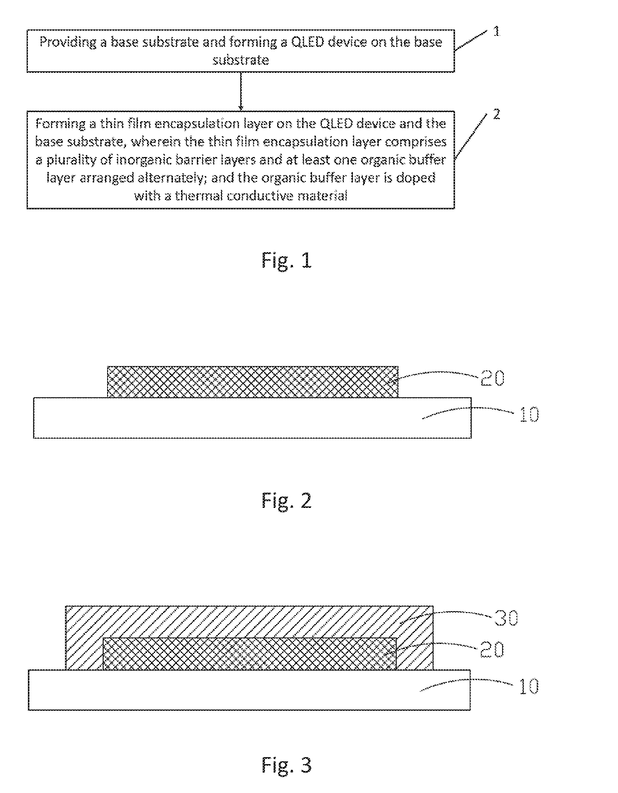
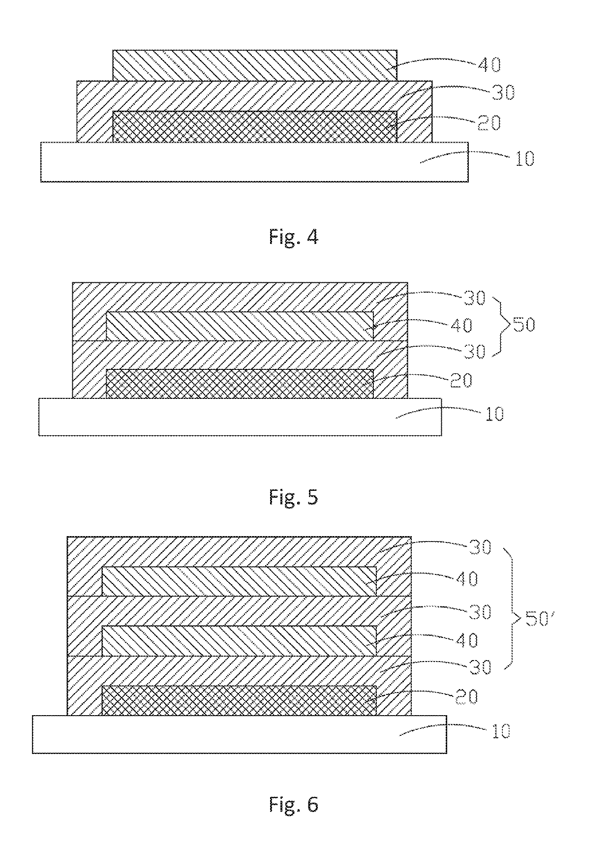
[0044]Please refer to FIG. 1 to FIG. 5, the present disclosure provides a method for packaging a QLED device, including the following steps:

[0045]Step 1, as shown in FIG. 2, providing a base substrate 10, a forming a QLED device 20 on the base substrate 10.

[0046]Specifically, the base substrate 10 is a TFT substrate and includes a plurality of thin film transistors (not shown) arrayed to drive the QLED device 20 to emit light.

[0047]Step 2, as shown in FIG. 3 to FIG. 6, forming a thin film encapsulation layer 50 on the QLED device 20 and the base substrate 10; wherein the thin film encapsulation layer 50 includes a plurality of inorganic barrier layers 30 and at least one organic buffer layer 40 arranged alternately; and the organic buffer layer 40 is doped with a ...


PUM


Abstract

The present disclosure provides a packaging method and a package structure of a QLED device. The packaging method of the QLED device forming a thin film encapsulation layer in which a plurality of inorganic barrier layers and at least one organic buffer layer are arranged alternately on a QLED device to seal the QLED device against water and oxygen, and the organic buffer layer is further doped with a thermal conducting material, so that the heat generated by the QLED device can be promptly transmitted through the thin film encapsulation layer to improve the heat dissipation of the thin film encapsulation layer, thereby improving the light extraction efficiency and the service life of the QLED device.

Description

RELATED APPLICATIONS[0001]The present application is a National Phase of International Application Number PCT / CN2017 / 110991, filed on Nov. 15, 2017, and claims the priority of China Application No. 201710931768.4, filed on Oct. 9, 2017.FIELD OF THE DISCLOSURE[0002]The present disclosure relates to a display device packaging field, and more particularly to a packaging method and a package structure of a QLED device.BACKGROUND OF THE DISCLOSURE[0003]Organic Light Emitting Display (OLED) has the advantages of self-luminous, low driving voltage, high luminous efficiency, short response time, sharpness and contrast, nearly 180° viewing angle, wide temperature range, flexible display and large-area full-color display. It is recognized as the most promising display device in the industry.[0004]The lighting principle of the OLED device is: the semiconductor material and the organic light emitting material cause light emission through the carrier injection and recombination driven by the ele...

Claims


Application Information

Patent Timeline
IPC IPC(8): H01L33/56H01L33/64H01L33/06
CPCH01L2933/0075H01L33/56H01L33/641H01L33/06H01L27/15H01L2933/005H01L33/644H10K50/115H10K50/8445H10K50/87H10K50/80
Inventor XIAO, YADANJIAO, SHIBO
Owner SHENZHEN CHINA STAR OPTOELECTRONICS SEMICON DISPLAY TECH CO LTD
Why Eureka
Try Eureka